Find a component by marking. smd transistors
Diode marking
Marking output diodes:
The most common coding systems are:
- JEDEC(USA)- Standardized EIA370 N-series numbering system.
Code view: <цифра><буква><serial number>[suffix].
The first digit is a digit reflecting the number of transitions in the element (1 for diodes).
The letter is always the letter "N".
The serial number is a two-, three-, or four-digit number that reflects the serial number of the semiconductor device's registration with the EIA.
Suffix - reflects the breakdown of devices of the same type into different nominal ratings according to characteristic parameters. A suffix can be one or more letters.
For example: 1N34A/1N270 (germanium diode), 1N914/1N4148 (silicon diode), 1N4001-1N4007 (1A silicon rectifier diode), and 1N54xx (3A power silicon rectifier diode).
- PRO ELECTRON (Europe);
The designation consists of four elements.
The first element is a letter indicating the type of semiconductor material used in the device:
- A - germanium;
- B - silicon;
- C - gallium arsenide;
- R - other semiconductor materials.
The second element is a letter indicating the type of semiconductor device:
- A - low-power pulse and universal diodes;
- B - varicaps;
- E - tunnel diodes;
- G - devices for special purposes (for example, generators), as well as complex devices containing several different components in one case;
- H - magnetically sensitive diodes;
- P - photosensitive devices (photodiodes, phototransistors, etc.);
- Q - light-emitting devices (LEDs, IR diodes, etc.);
- X - multiplying diodes;
- Y - rectifier diodes, boosters;
The third element is a letter, which is put only for devices intended for use in special-purpose equipment (industrial, professional, military, etc.). Usually the letters “Z”, “Y”, “X” or “W” are used. In the designations of general-purpose devices, this element is absent.
The fourth element is the two-, three-, or four-digit instrument serial number.
The designation may contain some additional elements. For example, the suffix is the same as in the JEDEC system, which reflects the breakdown of devices of the same type into different nominal ratings according to characteristic parameters.
For some instrument types (such as zener diodes) an additional classification may apply. In this case, an additional code is added to the main designation (it can also be through a hyphen or a fraction). For example, an additional code is often used containing information about the stabilization voltage and its possible spread (“A” - 1%, “B” - 2%, “C” - 5%, “D” - 10%, “E” - 15 %). If the stabilization voltage is not an integer, then the letter V is put instead of a comma. additional code for rectifier diodes, the maximum reverse voltage amplitude is indicated.
For example, BZY88C4V7 is a special-purpose silicon zener diode with registration number 88, a stabilization voltage of 4.7 V with a maximum deviation of this voltage from the nominal value of ± 5%.
Table 1 - Color coding of diodes (PRO ELECTRON).
- JIS (Japan, Asia);
The designation consists of five elements.
The first element is a number reflecting the number of transitions in the element (0 - photodiodes; 1 - diodes).
The second element is the letter “S”, denoting semiconductor devices (Semiconductors).
The third element is a letter indicating the type of semiconductor device:
- E - diodes;
- G - Gunn diodes;
- Q - light emitting diodes;
- R - rectifier diodes;
- S - low-current diodes;
- T - avalanche diodes;
- V - varicaps, p-i-n-diodes, diodes with charge accumulation;
- Z - zener diodes, limiters.
The fourth element is the serial (registration) number of the device.
The fifth element is a modification of the device (“A” - the first, “B” - the second, etc.).
After the standard marking, an additional index (“N”, “M”, “S”) may follow, reflecting some special properties of the device.
 Table 2 - Color coding of diodes (JIS-C-7012 and JEDEC).
 Marking of SMD diodes:
SMD diodes are usually marked with an alphanumeric code. Depending on the type of housing (i.e. its size) and the manufacturer, one or another coding system is used. It is quite obvious that it is not possible to consider all types of coding. Therefore, some codes for the most commonly used diode packages will be considered below. More full version you can look at coding systems for SMD diodes.
For SOD80 (MiniMELF) packages:
 Table 3 - Coding of SMD diodes in the SOD80 package.
 Example: BZV87-1V4 - silicon zener diode for a stabilization voltage of 1.4 V.
The remaining values of the zener diodes are encoded in a similar way.
Color coding:
 Table 4 - Color coding of SMD diodes in the SOD80 package.
 Often the manufacturer encodes only the type of diode:
 Table 5 - Color coding type of SMD diodes.
 For casesSOT89:
 Table 6 - Coding of SMD diodes in the SOT89 package.
 For cases SOD123, SOD323:
 Table 7 - Color coding of SMD diodes in SOD123 and SOD32 packages.
 Conventional designation of diodes on the diagrams
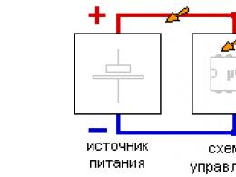
 Figure 7 - Designation of the terminals of the diode.
  Figure 8 - UGO diodes.
 Next to the symbol, the element type (VD) and serial number are indicated.
We have already got acquainted with the main radio components: resistors, capacitors, diodes, transistors, microcircuits, etc., and also studied how they are mounted on a printed circuit board. Let us once again recall the main stages of this process: the conclusions of all components are passed into the holes available in printed circuit board. After that, the conclusions are cut off, and then with reverse side boards are soldered (see Fig. 1).
This process already known to us is called DIP editing. This installation is very convenient for beginner radio amateurs: the components are large, you can solder them even with a large “Soviet” soldering iron without the help of a magnifying glass or microscope. That is why all Master Kits for self-soldering involve DIP mounting.
Rice. 1. DIP mounting
But DIP editing has very significant disadvantages:
Large radio components are not suitable for creating modern miniature electronic devices;
- output radio components are more expensive to manufacture;
- PCB for DIP-mounting is also more expensive due to the need to drill many holes;
- DIP mounting is difficult to automate: in most cases, even in large electronics factories, installation and soldering of DIP parts must be done manually. It is very expensive and time consuming.
Therefore, DIP-mounting is practically not used in the production of modern electronics, and it was replaced by the so-called SMD-process, which is the standard of today. Therefore, any radio amateur should have at least a general idea about it.
SMD mounting
SMD components (chip components) are electronic circuit components applied to a printed circuit board using surface mount technology - SMT technology (Eng. surface mount technology). That is, all electronic elements that are “fixed” on the board in this way are called smd components(English) surface mounted device). The process of mounting and soldering chip components is properly called the SMT process. It is not entirely correct to say “SMD-assembly”, but in Russia this version of the name of the technical process has taken root, so we will say the same.
On fig. 2. shows a section of the SMD mounting board. The same board, made on DIP-elements, will have several times larger dimensions.

Fig.2. SMD mounting
SMD mounting has undeniable advantages:
Radio components are cheap to manufacture and can be arbitrarily miniature;
- printed circuit boards are also cheaper due to the lack of multiple drilling;
- installation is easy to automate: installation and soldering of components is carried out by special robots. There is also no such technological operation as trimming the leads.
SMD resistors
Acquaintance with chip components is most logical to start with resistors, as with the simplest and most massive radio components.
The SMD resistor in terms of its physical properties is similar to the “usual”, output version we have already studied. All its physical parameters (resistance, accuracy, power) are exactly the same, only the case is different. The same rule applies to all other SMD components.

Rice. 3. CHIP resistors
Sizes of SMD resistors
We already know that output resistors have a certain grid of standard sizes, depending on their power: 0.125W, 0.25W, 0.5W, 1W, etc.
Chip resistors also have a standard size grid, only in this case the size is indicated by a four-digit code: 0402, 0603, 0805, 1206, etc.
The main sizes of resistors and their specifications shown in Fig.4.

Rice. 4 Main sizes and parameters of chip resistors
Marking SMD resistors
Resistors are marked with a code on the case.
If there are three or four digits in the code, then the last digit means the number of zeros, in fig. 5. The resistor with the code "223" has the following resistance: 22 (and three zeros on the right) Ohm = 22000 Ohm = 22 kOhm. The resistor with the code "8202" has a resistance: 820 (and two zeros on the right) Ohm = 82000 Ohm = 82 kOhm.
In some cases, the marking is alphanumeric. For example, a resistor coded 4R7 has a resistance of 4.7 ohms, and a resistor coded 0R22 has a resistance of 0.22 ohms (here, the letter R is the separator character).
There are also resistors of zero resistance, or jumper resistors. Often they are used as fuses.
Of course, you can not remember the code designation system, but simply measure the resistance of the resistor with a multimeter.

Rice. 5 Marking chip resistors
Ceramic SMD Capacitors
Externally, SMD capacitors are very similar to resistors (see Fig. 6.). There is only one problem: they do not have a capacitance code, so the only way to determine it is to measure it with a multimeter that has a capacitance measurement mode.
SMD capacitors are also available in standard sizes, usually similar to resistor sizes (see above).

Rice. 6. SMD ceramic capacitors
Electrolytic SMS Capacitors

Fig.7. Electrolytic SMS Capacitors
These capacitors are similar to their output counterparts, and the markings on them are usually explicit: capacitance and operating voltage. A strip on the "hat" of the capacitor marks its negative terminal.
SMD transistors

Fig.8. SMD transistor
Transistors are small, so it is impossible to write their full name on them. Are limited to code marking, and some international standard no designations. For example, the code 1E may indicate the type of transistor BC847A, or maybe some other. But this circumstance absolutely does not bother either manufacturers or ordinary consumers of electronics. Difficulties can only arise during repairs. Determining the type of transistor installed on a printed circuit board without the manufacturer's documentation for this board can sometimes be very difficult.
SMD Diodes and SMD LEDs
Photos of some diodes are shown in the figure below:

Fig.9. SMD Diodes and SMD LEDs
On the body of the diode, the polarity must be indicated in the form of a strip closer to one of the edges. Usually the cathode output is marked with a stripe.
The SMD LED also has a polarity, which is indicated either by a dot near one of the pins, or in some other way (you can find out more about this in the component manufacturer's documentation).
Define SMD type-diode or LED, as in the case of a transistor, is difficult: an uninformative code is stamped on the diode case, and most often there are no marks on the LED case at all, except for the polarity mark. Developers and manufacturers of modern electronics care little about its maintainability. It is understood that the repair of the printed circuit board will be a service engineer who has complete documentation for a particular product. Such documentation clearly describes where a particular component is installed on the printed circuit board.
Installation and soldering of SMD components
SMD assembly is optimized primarily for automatic assembly by special industrial robots. But amateur radio amateur designs can also be made on chip components: with sufficient accuracy and care, you can solder parts the size of a grain of rice with the most ordinary soldering iron, you only need to know some subtleties.
But this is a topic for a separate large lesson, so more details about automatic and manual SMD editing will be discussed separately.
If you looked into the insides of modern electronic device, then I probably noticed that the radio elements look completely different from those of equipment released 25-30 years ago. Conventional transistors, diodes, and ICs have replaced pinhead-sized parts soldered right on top of the board. Such parts, called SMD, are often as similar as two peas in a pod. How to distinguish one from the other and find out its type and purpose? Today we will talk about SMD diodes, zener diodes and their marking, and at the same time we will learn to distinguish one type of device from another.
What is SMD
First of all, what does "SMD" stand for and where does such a strange name come from? Everything is very simple: it is an abbreviation for the English expression Surface Mounted Device, which means a surface-mounted device. SMD diode (left), transistor and SMD LED
That is, unlike a conventional radio component, the legs of which are inserted into holes in the printed circuit board and soldered on its other side, the smd device is simply superimposed on the pads provided on the board and soldered on the same side.  Fragments of boards assembled using smd technology
Surface mount technology not only allowed to reduce the dimensions of the elements and the density of the elements on the board, but also significantly simplified the installation itself, which robots can easily handle today. The machine applies an electronic component to the required place on the board, heats up this place with IR light or laser to the melting temperature of the solder paste applied on the pads, and the element is assembled.
 Robot for smd editing
 Cases of SMD elements
Semiconductor devices intended for surface mounting are available in packages various types. For diodes and zener diodes, the main ones are: metal-glass cylindrical and plastic (ceramic) rectangular.
 SMD semiconductors in various types of packages
 Below I give the standard dimensions of SMD semiconductor packages, depending on the type.
Standard sizes of glass-to-metal imported SMD semiconductors
Type of shell | Overall length, mm | Width of contact pads, mm | Diameter, mm |
| DO-213AA (SOD80) | 3.5 | 0.48 | 1.65 |
| DO-213AB (MELF) | 5.0 | 0.48 | 2.52 |
| DO-213AC | 3.45 | 0.42 | 1.4 |
| ERD03LL | 1.6 | 0.2 | 1.0 |
| ERO21L | 2.0 | 0.3 | 1.25 |
| ERSM | 5.9 | 0.6 | 2.2 |
| MELF | 5.0 | 0.5 | 2.5 |
| SOD80 (miniMELF) | 3.5 | 0.3 | 1.6 |
| SOD80C | 3.6 | 0.3 | 1.52 |
| SOD87 | 3.5 | 0.3 | 2.05 |
Standard sizes of imported SMD semiconductors in plastic and ceramic cases
Type of shell | Length with leads, mm | Length withoutconclusions, mm | Width, mm | Height, mm | Output width, mm |
| DO-215AA | 6.2 | 4.3 | 3.6 | 2.3 | 2.05 |
| DO-215AB | 9.9 | 6.85 | 5.9 | 2.3 | 3.0 |
| DO-215AC | 6.1 | 4.3 | 2.6 | 2.4 | 1.4 |
| DO-215BA | 6.2 | 4.45 | 2.6 | 2.95 | 1.3 |
| ESC | 1.6 | 1.2 | 0.8 | 0.6 | 0.3 |
| SOD-123 | 3.7 | 2.7 | 1.55 | 1.35 | 0.6 |
| SOD-123 | 2.5 | 1.7 | 1.25 | 1.0 | 0.3 |
| SSC | 2.1 | 1.3 | 0.8 | 0.8 | 0.3 |
| SMA | 5.2 | 4.1 | 2.6 | — | 1.7 |
| SMB | 5.4 | 4.3 | 3.6 | — | 2.3 |
| SMC | 7.95 | 6.8 | 5.9 | — | 3.3 |

Expert opinion
Alexey Bartosh
Ask an expertIn fact, there are many more brands and types of SMD diodes and zener diodes. New ones appear faster than I type, with every reputable manufacturing company trying to introduce new standard and name it your own. The same can be said about labeling.
As for light-emitting SMD diodes (LEDs), everything is simpler. The actual dimensions of these devices correspond to their standard size. For example, it looks like a rectangle with dimensions of 2.8 x 3.5 mm, and 5050 - 5 x 5 mm.
 The actual dimensions of light emitting SMD diodes correspond to their designation
 SMD Semiconductor Marking
We figured out the cases, but after all, in a case of the same size there can be devices with completely different characteristics. How to determine what is in your hands? For this, one or another marking is applied, which is applied to the body of the device.
Diodes
SMD diodes in cylindrical packages are usually color-coded - they are marked with one or two colored stripes located at the cathode terminal.
imported color code tableSMD diodes in a cylindrical package
A similar marking is also used for diodes in a rectangular case:
Color codingSMD diodes in SOD-123 packages
* - the marking strip is located closer to the cathode terminal
Some manufacturers put symbols or numbers on their devices.
Symbol markingSMD diodes including Schottky diodes
Diode type | Marking |
| BAS16 | JU/A6 |
| BAS21 | JS |
| BAV70 | JJ/A4 |
| BAV99 | JK; JE; A |
| BAW56 | JD; A1 |
| BAT54S1 | L44 |
| BAT54C1 | L43 |
| BAV23S | L31 |
Semiconductor assemblies
Often, manufacturers build several diodes into one housing at once. This not only reduces the dimensions of the entire structure, but also simplifies installation. Such devices are called SMD assemblies. Depending on the type and purpose of the SMD assembly, it can consist of a very different number of semiconductors: from two to several dozen, and they can be interconnected in one way or another inside the SMD assembly itself.
For example, a very common connection of two Schottky diodes used in pulse rectifiers is anodes or cathodes. No less popular are ready-made SMD rectifier bridges, consisting of four semiconductors. Like conventional diodes, assemblies are marked accordingly.

BAV70 dual diode SMD assembly and bridge DB107GS — appearance and their wiring diagram
Such SMD devices are produced in SOT, TSOP SSOP packages and can have a different number of pins, which depends on the number of semiconductors and internal circuit their connections. I give the marking of the most popular assemblies below.
Marking semiconductor SMD assemblies from Hewlett Packard
| # | Tsokolevka | Assembly Composition | Type of shell |
| 2 | D1i | 2 diodes in series | SOT23 |
| 3 | D1j | 2 diodes common anode | SOT23 |
| 4 | D1h | 2 diodes common cathode | SOT23 |
| 5 | D6d | 2 diodes | SOT143 |
| 7 | D6c | 4 diodes included in the ring | SOT143 |
| 8 | D6a | diode bridge | SOT143 |
| FROM | D2b | 2 diodes | SOT323 |
| E | D2c | 2 diodes common anode | SOT323 |
| F | D2d | 2 diodes common cathode | SOT323 |
| K | D7b | 2 diodes | SOT363 |
| L | D7f | 3 diodes | SOT363 |
| M | D7g | 4 diodes common cathode | SOT363 |
| N | D7h | 4 diodes common anode | SOT363 |
| P | D7i | diode bridge | SOT363 |
| R | D7j | 4 diodes connected in a ring | SOT363 |
Marking of semiconductor SMD assemblies in SOT23 and SOT323 packages
Instrument type | Marking | Assembly Composition | Frame |
| BAV70 | JJ/A4 | 2 diodes | SOT23 |
| BAV99 | JK, JE, A7 | ||
| BAW56 | JD, A1 | ||
| BAT54S | L44 | 2 Schottky | |
| BAT54C | L43 | ||
| BAV70W | A4 | 2 diodes | SOT323 |
| BAV99W | A7 | ||
| BAW56W | A1 | ||
| BAT54AW | 42 | 2 Schottky | |
| BAT54CW | 43 | ||
| BAT54SW | 44 |
 According to the marking on the body of the device, we have a BAT54S assembly with Schottky semiconductors
 zener diodes
Zener diodes and diodes can have both color and symbol marking:
Color codingSMD zener diodes in a glass barrel
* - marking strips are located closer to the cathode terminal
Symbol markingSMD zener diodes BZX84 in a rectangular package
Instrument type | Marking | Stabilization voltage, V |
| BZX84C2V7 | W4 | 2.7 |
| BZX84C3V0 | W5 | 3.0 |
| BZX84C3V3 | W6 | 3.3 |
| BZX84C3V9 | W8 | 3.9 |
| BZX84C4V3 | Z0 | 4.3 |
| BZX84C4V7 | Z1 | 4.7 |
| BZX84C5V1 | Z2 | 5.1 |
| BZX84C5V6 | Z3 | 5.6 |
| BZX84C6V2 | Z4 | 6.2 |
| BZX84C6V8 | Z5 | 6.8 |
| BZX84C7V5 | Z6 | 7.5 |
| BZX84C8V2 | Z7 | 8.2 |
| BZX84C9V1 | Z8 | 9.1 |
| BZX84C10 | Z9 | 10.0 |
| BZX84C12 | Y2 | 12.0 |
| BZX84C15 | Y4 | 15.0 |
| BZX84C18 | Y6 | 18.0 |
| BZX84C20 | Y8 | 20.0 |
Symbol markingSMD zener diodes BZT52 in a rectangular package
LEDs
Marking on SMD LEDs is usually not affixed (an exception may be fakes - they are often marked for greater credibility), and their digital designation only indicates the size of the device. All other information can be found in the documentation that comes with SMD LEDs, or from the table below:
Main characteristicsSMD LEDs of various types
Instrument type | Power, W | Luminous flux, lm | Dimensions, mm |
| 2828 | 0.5 | 50 | 2.8x2.8 |
| 2835(a) | 0.2 | 29 | 2.8x3.5 |
| 2835(b); | 0.5 | 63 | 2.8x3.5 |
| 2835(c) | 1 | 130 | 2.8x3.5 |
| 3014 | 0.1 | 9-12 | 3.0 x 1.4 |
| 3020 | 0.06 | 5.4 | 3.0x2.0 |
| 3020(b) | 0.5 | 3.0x2.0 | |
| 3020(c) | 1 | 125 | 3.0x2.0 |
| 3030 | 0.9 | 110-120 | 3.0 x 3.0; |
| 3228 | 1 | 110 | 3.2 x 2.8 |
| 3258 | 0.2 | 6 | 3.2 x 5.8 |
| 3528(a) | 0.06 | 7 | 3.5x2.8 |
| 3528(b) | 1 | 110 | 3.5x2.8 |
| 3535(a) | 0.5 | 35-42 | 3.5 x 3.5 |
| 3535(b) | 1 | 110 | 3.5 x 3.5 |
| 3535(c) | 2 | 3.5 x 3.5 | |
| 4014 | 0.2 | 22-32 | 4.0x1.4 |
| 4020 | 0.5 | 55 | 4.0x2.0 |
| 5050 | 0.2 | 14-22 | 5.0x5.0 |
| 5060 | 0.2 | 26 | 5.0x6.0 |
| 5630 | 0.5 | 30-45 | 5.6 x 3.0 |
| 5730 | 0.5 | 30-45 | 5.7 x 3.0 |
| 5733 | 0.5 | 35-50 | 5.7 x 3.3 |
| 5736 | 0.5 | 40-55 | 5.7 x 3.6 |
| 7014(a) | 0.5 | 35-49 | 7.0 x 1.4 |
| 7014(b) | 1 | 110 | 7.0 x 1.4 |
| 7020 | 1 | 110 | 7.0x2.0 |
| 7020 | 0.5 | 40-55 | 7.0x2.0 |
| 7030 | 1 | 110 | 7.0x3.0 |
| 8520(a) | 0.5 | 55-60 | 8.5x2.0 |
| 8520(b) | 1 | 110 | 8.5x2.0 |
As can be seen from the plate, the 2835 device can be produced in three versions - 0.2, 0.5 and 1 W. Moreover, there are many fakes when craftsmen embed a crystal of any power - from 0.1 W and below into a case of size 2835. And to make the fake look more convincing, as I wrote above, crooks can even put a mark! It is impossible to determine what you really have in your hands either visually or by size. This can only be done according to the accompanying documentation and approximately at a price - the lower it is, the lower the power of the LED.
Expert opinion
Alexey Bartosh
Specialist in the repair, maintenance of electrical equipment and industrial electronics.
Ask an expertIn fact, with some experience, you can determine the approximate power of the LED without visual marking. The crystal is often seen through the compound with which it is filled. The larger the crystal, the more powerful the device.
But that's not all. An LED of the same size can have a different color temperature and even color. For the same 2835, the light can be warm, daylight and cold, and, for example, SMD 3020 can turn out to be of any glow color.
The 5050 is equipped with three crystals placed in one housing, and each of them can also have a different glow color. All this information is only in the accompanying documentation.
 LED 5050 with three crystals and LED Strip Light assembled on tri-color SMD 5050
 So our conversation about SMD semiconductors and their marking has ended. Now you know what they are, and if necessary, you can determine the type of SMD diode, zener diode or LED that you hold in your hands by marking.
There were circuits based on discrete electronic elements - resistors, transistors, capacitors, diodes, inductors, and they heated up during operation. And they still had to be cooled - a whole ventilation and cooling system was being built. There were no air conditioners anywhere, people endured the heat, and all the engine rooms were blown and cooled centrally and continuously, day and night. And the energy consumption went to megawatts. The computer's power supply occupied a separate cabinet. 380 volts, three phases, bottom connection, from under the raised floor. Another cabinet occupied the processor. Another one is random access memory on magnetic cores. And all together occupied a hall with an area of about 100 square meters. And the car had RAM, scary to say, 512 KB.
And it was necessary to make computers more powerful and more powerful.
Then LSI was invented - large integrated circuits. This is when the entire circuit is drawn in one solid form. A multilayered parallelepiped, in which layers of microscopic thickness contain the same electronic elements drawn, sprayed or welded in vacuum, only microscopic, and “crushed” into a plane. Usually a whole LSI is sealed in one case, and then it is not afraid of anything - a piece of iron, even hit with a hammer (just kidding).


Only LSI (or VLSI - very large integrated circuits) contain function blocks or separate electronic devices - processors, registers, semiconductor memory blocks, controllers, operational amplifiers. And the task is to assemble them into a specific product: mobile phone, flash drive, computer, navigator, etc. But they are so small, these BIG integrated circuits, how to assemble them?
And then came up with surface mount technology.
SMT/TMP complex electronic circuit assembly method
It soon became inconvenient and non-technological to assemble microchips, BISs, resistances, capacitors on the board in the old fashioned way. And installation according to the traditional "end-to-end" technology became cumbersome and difficult to automate, and the results were not in accordance with the realities of the time. Miniature gadgets require miniature and, most importantly, easy-to-layout boards. The industry can already produce resistors, transistors, etc., very small and very flat. The matter remained small - to make their contacts flat, pressed to the surface. And to develop a technology for tracing and manufacturing boards as the basis for surface mounting, as well as methods for soldering elements to the surface. In addition to other advantages, they learned how to solder as a whole - the entire board at once, which speeds up the work and gives uniformity in its quality. This method is called " T technology m mounting on P surface (TMP)”, or surface mount technology (SMT). Since the mounted elements have become completely flat, in everyday life they are called "chips", or "chip components" (or even SMD - surface mounted device, for example, SMD resistors).
TMP board manufacturing steps
The manufacture of a TMP board affects both the process of its design, manufacture, selection of certain materials, and specific technical means for soldering chips to the board.
- The design and manufacture of the board is the basis for the installation. Instead of holes for through mounting, contact pads are made for soldering the flat contacts of the elements.
- Applying solder paste to pads. This can be done with a syringe by hand or by screen printing in mass production.
- Precise installation of components on the board over the applied solder paste.
- Placing the board with all components in the soldering oven. The paste melts and very compactly (due to additives that increase the surface tension of the solder) solder the contacts with the same quality over the entire surface of the board. However, the requirements for both operation time, temperature, and the accuracy of the chemical composition of materials are critical.
- Finishing: cooling, washing, applying a protective layer.


There are different technology options for mass production and for manual production. Mass production, subject to extensive automation and subsequent quality control, gives and guaranteed high results.
However, SMT technology can also get along well with traditional mounting on a single board. In this case, manual SMT installation may be required.
SMD Resistors
The resistor is the most common component electronic circuits. There is even a specially designed circuitry, which is built only from transistors and resistors (T-R-logic). This means that without the remaining elements it is possible to build a processor, but without these two - in no way. (Sorry, there is also TT logic, where there are generally only transistors, but some of them have to play the role of resistors). It is in the production of large integrated circuits that they go to such extremes, but for surface mounting, the entire set of necessary elements is still produced.

For such a compact assembly, they must have strictly defined dimensions. Each SMD device is a small parallelepiped with contacts protruding from it - legs, or plates, or metal tips on both sides. It is important that the contacts on the mounting side must lie strictly in a plane, and on this plane have the area necessary for soldering - also rectangular.

Resistor dimensions: l - length, w - width, h - height. The standard dimensions are the length and width that are important for installation.
They can be encoded in one of two systems: inch (JEDEC) or metric (mm). The conversion factor from one system to another is the length of an inch with mm = 2.54.
Standard sizes are encoded with a four-digit digital code, where the first two digits are the length, the second are the width of the device. Moreover, the dimensions are taken either in hundredths of an inch, or in tenths of a millimeter, depending on the standard.
And code 1608 in the metric system means 1.6 mm long and 0.8 mm wide. By applying the conversion factor, it is easy to verify that these are the same standard size. However, there are other dimensions that are determined by the size.

Chip resistor marking, ratings
Due to the small area of the device for applying the usual rating for resistors, it was necessary to invent a special marking. There are two purely numeric - three-digit and four-digit) and two alphanumeric (EIA-96), in which two digits and a letter and an encoding for resistance values \u200b\u200bless than 0, which uses the letter R to indicate the position of the decimal point.
And there is another special marking. A "resistor" without any resistance, that is, just a metal jumper, is marked 0, or 000.

Digital markings
Numerical markings contain the index (N) of the multiplier (10 N) as the last digit, the other two or three are the resistance mantissa.
In general, the term SMD (from the English. Surface Mounted Device) can be attributed to any small-sized electronic component designed to be mounted on the surface of the board using SMT technology (surface mount technology).
SMT technology (from the English. Surface mount technology) was developed in order to reduce the cost of production, increase the efficiency of manufacturing printed circuit boards using smaller electronic components: resistors, capacitors, transistors, etc. Today we will consider one of these - SMD resistor.
SMD resistors
SMD resistors- These are miniature, designed for surface mounting. SMD resistors are significantly smaller than their traditional counterpart. They are often square, rectangular, or oval in shape, with a very low profile.
Instead of the wire leads of conventional resistors that are inserted into the holes of the printed circuit board, SMD resistors there are small contacts that are soldered to the surface of the resistor housing. This eliminates the need to make holes in the printed circuit board, and thus allows more efficient use of its entire surface.
Sizes of SMD resistors
Basically, the term frame size includes the size, shape, and pin configuration (package type) of an electronic component. For example, the configuration of a conventional chip that has a flat, double-sided pinout package (perpendicular to the plane of the base) is called a DIP.
Size of SMD resistors are standardized and most manufacturers use the JEDEC standard. The size of SMD resistors is indicated by a numerical code, for example, 0603. The code contains information about the length and width of the resistor. So in our example, code 0603 (in inches), the case is 0.060 inches long by 0.030 inches wide.
The same size resistor in the metric system will have code 1608 (in millimeters), respectively, the length is 1.6 mm, the width is 0.8 mm. To convert the dimensions to millimeters, it is enough to multiply the size in inches by 2.54.
Sizes of SMD resistors and their power
The size of the SMD resistor depends mainly on the required power dissipation. The following table lists the sizes and specifications of the most commonly used SMD resistors.

Marking SMD resistors
Due to the small size of SMD resistors, it is almost impossible to apply traditional color coding resistors.
In this regard, a special marking method was developed. The most common marking contains three or four numbers, or two numbers and a letter, which has the name EIA-96.
Marking with 3 and 4 digits
In this system, the first two or three digits indicate the numerical value of the resistance of the resistor, and the last digit indicates the multiplier. This last digit indicates the power to which 10 must be raised to get the final multiplier.


A few more examples of determining resistance within this system:
- 450 \u003d 45 x 10 0 is equal to 45 ohms
- 273 \u003d 27 x 10 3 is equal to 27000 ohms (27 kOhm)
- 7992 \u003d 799 x 10 2 is equal to 79900 ohms (79.9 kOhm)
- 1733 \u003d 173 x 10 3 is equal to 173000 ohms (173 kOhm)
The letter “R” is used to indicate the position of the decimal point for resistance values below 10 ohms. Thus, 0R5 = 0.5 ohm and 0R01 = 0.01 ohm.

SMD resistors of increased accuracy (precision) in combination with small sizes have created a need for a new, more compact marking. In this regard, the EIA-96 standard was created. This standard designed for resistors with a resistance tolerance of 1%.

This marking system consists of three elements: two digits indicate the code, and the letter following them determines the multiplier. The two digits are a code that gives a three-digit resistance number (see table)
For example, code 04 means 107 ohms and 60 means 412 ohms. The multiplier gives the final value of the resistor, for example:
- 01A = 100 ohm ±1%
- 38C = 24300 Ohm ±1%
- 92Z = 0.887 ohm ±1%

Online SMD resistor calculator
This calculator will help you find the resistance value of SMD resistors. Just enter the code written on the resistor and its resistance will be displayed at the bottom.
The calculator can be used to determine the resistance of SMD resistors that are marked with 3 or 4 digits, as well as according to the EIA-96 standard (2 digits + letter).
While we have done our best to test the function of this calculator, we cannot guarantee that it calculates the correct values for all resistors, as sometimes manufacturers may use their own custom codes.
Therefore, to be absolutely sure of the resistance value, it is best to additionally measure the resistance with a multimeter.