Kinds and types of smd elements. SMD marking
We have already got acquainted with the main radio components: resistors, capacitors, diodes, transistors, microcircuits, etc., and also studied how they are mounted on a printed circuit board. Once again, let's recall the main stages of this process: the leads of all components are passed into the holes available in the printed circuit board. After that, the conclusions are cut off, and then with reverse side boards are soldered (see Fig. 1).
This process already known to us is called DIP editing. This installation is very convenient for beginner radio amateurs: the components are large, you can solder them even with a large “Soviet” soldering iron without the help of a magnifying glass or microscope. That is why all Master Kits for self-soldering involve DIP mounting.
Rice. 1. DIP mounting
But DIP editing has very significant disadvantages:
Large radio components are not suitable for creating modern miniature electronic devices;
- output radio components are more expensive to manufacture;
- PCB for DIP-mounting is also more expensive due to the need to drill many holes;
- DIP mounting is difficult to automate: in most cases, even in large electronics factories, installation and soldering of DIP parts must be done manually. It is very expensive and time consuming.
Therefore, DIP-mounting is practically not used in the production of modern electronics, and it was replaced by the so-called SMD-process, which is the standard of today. Therefore, any radio amateur should have at least a general idea about it.
SMD mounting
SMD components(chip components) are components electronic circuit printed on a printed circuit board using surface mount technology - SMT technology (Eng. surface mount technology). That is, all electronic elements that are “fixed” on the board in this way are called smd components(English) surface mounted device). The process of mounting and soldering chip components is properly called the SMT process. It is not entirely correct to say “SMD-assembly”, but in Russia this version of the name of the technical process has taken root, so we will say the same.
On fig. 2. shows a section of the SMD mounting board. The same board, made on DIP-elements, will have several times larger dimensions.

Fig.2. SMD mounting
SMD mounting has undeniable advantages:
Radio components are cheap to manufacture and can be arbitrarily miniature;
- printed circuit boards are also cheaper due to the lack of multiple drilling;
- installation is easy to automate: installation and soldering of components is carried out by special robots. There is also no such technological operation as trimming the leads.
SMD resistors
Acquaintance with chip components is most logical to start with resistors, as with the simplest and most massive radio components.
The SMD resistor in terms of its physical properties is similar to the “usual”, output version we have already studied. All its physical parameters (resistance, accuracy, power) are exactly the same, only the case is different. The same rule applies to all other SMD components.

Rice. 3. CHIP resistors
Sizes of SMD resistors
We already know that output resistors have a certain grid of standard sizes, depending on their power: 0.125W, 0.25W, 0.5W, 1W, etc.
Chip resistors also have a standard size grid, only in this case the size is indicated by a four-digit code: 0402, 0603, 0805, 1206, etc.
The main sizes of resistors and their specifications shown in Fig.4.
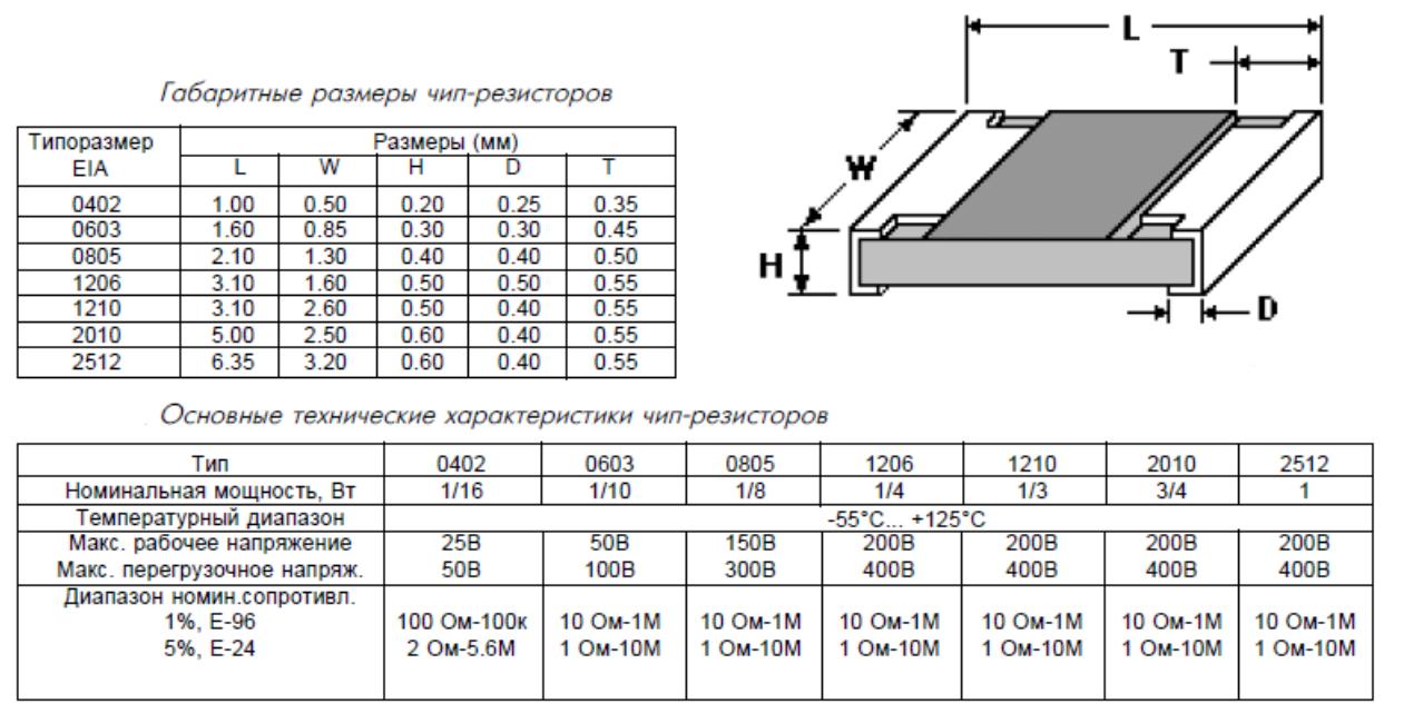
Rice. 4 Main sizes and parameters of chip resistors
SMD marking-resistors
Resistors are marked with a code on the case.
If there are three or four digits in the code, then the last digit means the number of zeros, in fig. 5. The resistor with the code "223" has the following resistance: 22 (and three zeros on the right) Ohm = 22000 Ohm = 22 kOhm. The resistor with the code "8202" has a resistance: 820 (and two zeros on the right) Ohm = 82000 Ohm = 82 kOhm.
In some cases, the marking is alphanumeric. For example, a resistor coded 4R7 has a resistance of 4.7 ohms, and a resistor coded 0R22 has a resistance of 0.22 ohms (here, the letter R is the separator character).
There are also resistors of zero resistance, or jumper resistors. Often they are used as fuses.
Of course, you can not remember the code designation system, but simply measure the resistance of the resistor with a multimeter.

Rice. 5 Marking chip resistors
Ceramic SMD Capacitors
Externally, SMD capacitors are very similar to resistors (see Fig. 6.). There is only one problem: they do not have a capacitance code, so the only way to determine it is to measure it with a multimeter that has a capacitance measurement mode.
SMD capacitors are also available in standard sizes, usually similar to resistor sizes (see above).

Rice. 6. SMD ceramic capacitors
Electrolytic SMS Capacitors

Fig.7. Electrolytic SMS Capacitors
These capacitors are similar to their output counterparts, and the markings on them are usually explicit: capacitance and operating voltage. A strip on the "hat" of the capacitor marks its negative terminal.
SMD transistors

Fig.8. SMD transistor
Transistors are small, so it is impossible to write their full name on them. Are limited to code marking, and some international standard no designations. For example, the code 1E may indicate the type of transistor BC847A, or maybe some other. But this circumstance absolutely does not bother either manufacturers or ordinary consumers of electronics. Difficulties can only arise during repairs. Determining the type of transistor installed on a printed circuit board without the manufacturer's documentation for this board can sometimes be very difficult.
SMD Diodes and SMD LEDs
Photos of some diodes are shown in the figure below:

Fig.9. SMD Diodes and SMD LEDs
On the body of the diode, the polarity must be indicated in the form of a strip closer to one of the edges. Usually the cathode output is marked with a stripe.
The SMD LED also has a polarity, which is indicated either by a dot near one of the pins, or in some other way (you can find out more about this in the component manufacturer's documentation).
It is difficult to determine the type of SMD diode or LED, as in the case of a transistor: an uninformative code is stamped on the diode case, and most often there are no marks on the LED case at all, except for the polarity mark. Developers and manufacturers of modern electronics care little about its maintainability. It is understood that the repair of the printed circuit board will be a service engineer who has complete documentation for a particular product. Such documentation clearly describes where a particular component is installed on the printed circuit board.
Installation and soldering of SMD components
SMD assembly is optimized primarily for automatic assembly by special industrial robots. But amateur radio amateur designs can also be made on chip components: with sufficient accuracy and care, you can solder parts the size of a grain of rice with the most ordinary soldering iron, you only need to know some subtleties.
But this is a topic for a separate large lesson, so more details about automatic and manual SMD editing will be discussed separately.
In our turbulent age of electronics, the main advantages of an electronic product are small dimensions, reliability, ease of installation and dismantling (equipment disassembly), low energy consumption and convenient usability ( from English- the convenience of use). All these advantages are by no means possible without surface mount technology - SMT technology ( S face M ount T echnology), and of course, without SMD components.
What are SMD components
SMD components are used in absolutely all modern electronics. SMD ( S face M ounted D evice), which is translated from English as “surface-mounted device”. In our case, the surface is a printed circuit board, without through holes for radio elements:
In this case, SMD components are not inserted into the board holes. They are soldered onto the contact tracks, which are located directly on the surface of the printed circuit board. In the photo below, there are tin-colored contact pads on the board of a mobile phone that used to have SMD components.

Advantages of SMD components
The biggest advantage of SMD components is their small size. In the photo below, simple resistors and:


Due to the small dimensions of SMD components, developers have the opportunity to place large quantity components per unit area than simple output radioelements. Consequently, the mounting density increases and, as a result, the dimensions of electronic devices are reduced. Since the weight of the SMD component is several times lighter than the weight of the same simple output radio element, the mass of the radio equipment will also be many times lighter.

SMD components are much easier to desolder. For this we need a hair dryer. How to solder and solder SMD components, you can read in the article how to solder SMD correctly. Soldering them is much more difficult. In factories, they are placed on a printed circuit board by special robots. No one welds them manually in production, except for radio amateurs and radio equipment repairmen.
Multilayer boards
Since in equipment with SMD components there is a very dense installation, there should be more tracks in the board. Not all tracks fit on the same surface, so printed circuit boards make multilayer. If the equipment is complex and has a lot of SMD components, then there will be more layers in the board. It's like a layered cake. The printed tracks connecting the SMD components are located right inside the board and cannot be seen in any way. An example of multilayer boards are boards mobile phones, boards of computers or laptops ( motherboard, video card, RAM etc).
In the photo below, the blue board is Iphone 3g, the green board is the computer motherboard.


All radio repairers know that if you overheat a multilayer board, it will swell up with a bubble. In this case, the interlayer connections are torn and the board becomes unusable. Therefore, the main trump card when replacing SMD components is the right temperature.
On some boards, both sides of the printed circuit board are used, while the mounting density, as you understand, is doubled. This is another plus of SMT technology. Oh yes, it is also worth considering the fact that the material for the production of SMD components takes many times less, and their cost in mass production in millions of pieces costs, literally, a penny.
Main types of SMD components
Let's look at the main SMD elements used in our modern devices. Resistors, capacitors, low-value inductors, and other components look like ordinary small rectangles, or rather, parallelepipeds))

On boards without a circuit, it is impossible to know whether it is a resistor, or a capacitor, or even a coil. The Chinese mark as they want. On large SMD elements, they still put a code or numbers to determine their belonging and denomination. In the photo below, these elements are marked in a red rectangle. Without a diagram, it is impossible to say what type of radio elements they belong to, as well as their denomination.

Sizes of SMD components can be different. Here is a description of the sizes for resistors and capacitors. Here, for example, is a rectangular yellow SMD capacitor. They are also called tantalum or simply tantalum:

And this is what SMD looks like:


There are other types SMD transistors:

Which have a large denomination, in the SMD version they look like this:


And of course, how could it be without microcircuits in our age of microelectronics! There are a lot of SMD chip package types, but I mainly divide them into two groups:
1) Microcircuits, in which the leads are parallel to the printed circuit board and are located on both sides or along the perimeter.

2) Microcircuits, in which the conclusions are located under the microcircuit itself. This is a special class of microcircuits called BGA (from English ball grid array- an array of balls). The conclusions of such microcircuits are simple solder balls of the same size.
In the photo below, the BGA microcircuit and its reverse side, consisting of ball leads.

BGA chips are convenient for manufacturers in that they greatly save space on the printed circuit board, because there can be thousands of such balls under any BGA chip. This greatly simplifies the life of manufacturers, but does not make life easier for repairmen.
Summary
What do you use in your designs? If your hands are not shaking, and you want to make a small radio bug, then the choice is obvious. But still, in amateur radio designs, dimensions do not particularly play a big role, and soldering massive radio elements is much easier and more convenient. Some radio amateurs use both. Every day more and more new chips and SMD components are being developed. Smaller, thinner, more reliable. The future, unambiguously, belongs to microelectronics.
A resistor is an element that has some kind of resistance and is used in electronics and electrical engineering to limit current or obtain the necessary voltages (for example, using a resistive divider). SMD resistors are surface mount resistors, in other words, mounting on the surface of a printed circuit board.
The main characteristics for resistors are the nominal resistance, measured in ohms and depends on the thickness, length and materials of the resistive layer, as well as the power dissipation.
Electronic components for surface mounting are small in size due to the fact that they either do not have terminals for connection in the classical sense. Elements for volumetric mounting have long leads.
Previously, when assembling electronic equipment, they connected the components of the circuit to each other (hinged mounting) or threaded them through the printed circuit board into the appropriate holes. Structurally, their conclusions or contacts are made in the form of metallized areas on the body of the elements. In the case of microcircuits and surface-mount transistors, the elements have short rigid "legs".
One of the main characteristics of SMD resistors is the size. This is the value of the length and width of the case, according to these parameters, elements are selected that correspond to the layout of the board. Usually, dimensions in the documentation are written in abbreviated four-digit numbers, where the first two digits indicate the length of the element in mm, and the second pair of characters indicate the width in mm. However, in fact, the dimensions may differ from the markings depending on the types and series of elements.
Typical sizes of SMD resistors and their parameters

Figure 1 - designations for decoding standard sizes.
1. SMD resistors 0201 :
L=0.6mm; W=0.3mm; H=0.23mm; L1=0.13 m.
Rated power: 0.05W
Working voltage: 15V
Maximum allowable voltage: 50 V
2. SMD resistors 0402 :
L=1.0mm; W=0.5mm; H=0.35mm; L1=0.25 mm.
Rating range: 0 ohm, 1 ohm - 30 MΩ
Permissible deviation from the nominal value: 1% (F); 5% (J)
Rated power: 0.062W
Working voltage: 50V
Operating temperature range: -55 - +125 °С
3. SMD resistors 0603 :
L=1.6mm; W=0.8mm; H=0.45mm; L1=0.3 mm.
Rating range: 0 ohm, 1 ohm - 30 MΩ
Permissible deviation from the nominal value: 1% (F); 5% (J)
Rated power: 0.1W
Working voltage: 50V
Maximum allowable voltage: 100 V
Operating temperature range: -55 - +125 °С
4. SMD resistors 0805 :
L=2.0mm; W=1.2mm; H=0.4mm; L1=0.4 mm.
Rating range: 0 ohm, 1 ohm - 30 MΩ
Permissible deviation from the nominal value: 1% (F); 5% (J)
Rated power: 0.125W
Working voltage: 150V
Maximum allowable voltage: 200 V
Operating temperature range: -55 - +125 °С
5. SMD resistors 1206 :
L=3.2mm; W=1.6mm; H=0.5mm; L1=0.5 mm.
Rating range: 0 ohm, 1 ohm - 30 MΩ
Permissible deviation from the nominal value: 1% (F); 5% (J)
Rated power: 0.25W
Working voltage: 200V
Operating temperature range: -55 - +125 °С
6. SMD resistors 2010 :
L=5.0mm; W=2.5mm; H=0.55mm; L1=0.5 mm.
Rating range: 0 ohm, 1 ohm - 30 MΩ
Permissible deviation from the nominal value: 1% (F); 5% (J)
Rated power: 0.75W
Working voltage: 200V
Maximum allowable voltage: 400 V
Operating temperature range: -55 - +125 °С
7. SMD resistors 2512 :
L=6.35mm; W=3.2mm; H=0.55mm; L1=0.5 mm.
Rating range: 0 ohm, 1 ohm - 30 MΩ
Permissible deviation from the nominal value: 1% (F); 5% (J)
Rated power: 1W
Working voltage: 200V
Maximum allowable voltage: 400 V
Operating temperature range: -55 - +125 °С
As you can see, with an increase in the size of the chip resistor, the nominal power dissipation also increases in the table below, this dependence is more clearly shown, as well as the geometric dimensions of resistors of other types:
Table 1 - Marking SMD resistors

Depending on the size, one of three types of marking of the resistor value can be used. There are three types of markings:
1. With 3 digits. In this case, the first two indicate the number of ohms, and the last number of zeros. This is how resistors from the E-24 series are marked, with a deviation from the nominal value (tolerance) of 1 or 5%. The size of resistors with this marking is 0603, 0805 and 1206. An example of such marking: 101 \u003d 100 \u003d 100 Ohm

Figure 2 is an image of a 10,000 ohm SMD resistor, aka 10 kOhm.
2. With 4 characters. In this case, the first 3 digits indicate the number of ohms, and the last - the number of zeros. This is how resistors from the E-96 series of sizes 0805, 1206 are described. If the letter R is present in the marking, it plays the role of a comma separating integers from fractions. Thus, the marking 4402 stands for 44,000 ohms or 44 kOhm.

Figure 3 - image of an SMD resistor with a nominal value of 44 kOhm
3. Marking with a combination of 3 characters - numbers and letters. In this case, the first 2 characters are numbers, they indicate the encoded resistance value in Ohms. The third character is the multiplier. In this way, resistors of size 0603 from the E-96 series of resistances are marked, with a tolerance of 1%. Translation of letters into a multiplier is performed in a row: S=10^-2; R=10^-1; B=10; C=10^2; D=10^3; E=104; F=10^5.
The decoding of the codes (the first two characters) is carried out according to the table shown below.
Table 2 - decoding of marking codes for SMD resistors


Figure 4 - a resistor with a three-character marking 10C, if you use the table and the given series of factors, then 10 is 124 Ohms, and C is a factor of 10 ^ 2, which equals 12,400 Ohms or 12.4 kOhm.
Basic parameters of resistors
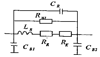
Figure 5 - Equivalent Circuit resistor
So, inductance and capacitance are elements that affect the impedance and the fronts of currents and voltages depending on frequency. The best in terms of frequency characteristics are the elements for surface mounting, due to their small size.

Figure 6 - The graph shows the ratio of the total resistance of the resistor to the active one at various frequencies
Resistor design
Surface mount resistors are cheap and convenient for assembly line automated assembly of electronic devices. However, they are not as simple as they might seem.
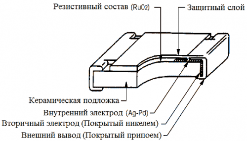
Figure 7 - Internal organization SMD resistor
The basis of the resistor is a substrate of Al2O3 - aluminum oxide. It is a good dielectric and a material with good thermal conductivity, which is no less important, since during operation the entire power of the resistor is released into heat.
As a resistive layer, a thin metal or oxide film is used, for example, chromium, ruthenium dioxide (as shown in the figure above). The characteristics of the resistors depend on the material of which this film is composed. The resistive layer of individual resistors is a film up to 10 µm thick, made of a material with a low TCR ( temperature coefficient resistance), which gives high temperature stability of the parameters and the ability to create high-precision elements, an example of such a material is constantan, however, the values of such resistors rarely exceed 100 ohms.
The contact pads of the resistor are formed from a set of layers. The inner contact layer is made of expensive materials like silver or palladium. Intermediate - nickel. And the outer one is lead-tin. This design is due to the need to ensure high adhesion (cohesion) of the layers. The reliability of contacts and noise depend on them.
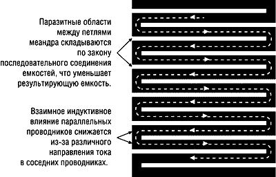
Figure 8 - shape of the resistive layer
The installation of such elements takes place in furnaces, and in amateur radio workshops using a blow dryer, that is, a stream of hot air. Therefore, in their manufacture, attention is paid to the temperature curve of heating and cooling.

Figure 9 - heating and cooling curve when soldering SMD resistors
conclusions
The use of surface-mounted components had a positive effect on the weight and size indicators of electronic equipment, as well as on frequency characteristics element. Modern industry produces most of the common elements in the SMD version. Including: resistors, capacitors, diodes, LEDs, transistors, thyristors, integrated circuits.
- Introduction
- SMD Component Enclosures
- Sizes of SMD components
- SMD resistors
- SMD Capacitors
- SMD coils and chokes
- SMD transistors
- Marking SMD components
- Soldering SMD components
Introduction
Not only ordinary components with leads are now available to a modern radio amateur, but also such small, dark ones, on which one cannot understand what is written, details. They are called "SMD". In Russian it means "surface mount components". Their main advantage is that they allow the industry to assemble boards using robots that place SMD components at great speed in their places on printed circuit boards, and then massively "bake" and receive assembled printed circuit boards as a result. On the part of the person are those operations that the robot cannot perform. Not yet.
The use of chip components in amateur radio practice is also possible, even necessary, as it allows to reduce the weight, size and cost of the finished product. Plus, you don't have to drill at all.
For those who first encountered SMD components, confusion is natural. How to understand their diversity: where is the resistor, and where is the capacitor or transistor, what sizes do they come in, what cases of smd parts exist? You will find answers to all these questions below. Read on, it's useful!
Chip component housings
Rather conventionally, all surface-mounted components can be divided into groups according to the number of pins and package size:
| pins/size | Very very small | Very small | small | Medium |
| 2 pins | SOD962 (DSN0603-2), WLCSP2*, SOD882 (DFN1106-2) , SOD882D (DFN1106D-2) , SOD523, SOD1608 (DFN1608D-2) | SOD323, SOD328 | SOD123F, SOD123W | SOD128 |
| 3 pins | SOT883B (DFN1006B-3) , SOT883, SOT663, SOT416 | SOT323, SOT1061 (DFN2020-3) | SOT23 | SOT89, DPAK (TO-252) , D2PAK (TO-263) , D3PAK (TO-268) |
| 4-5 pins | WLCSP4*, SOT1194, WLCSP5*, SOT665 | SOT353 | SOT143B, SOT753 | SOT223, POWER-SO8 |
| 6-8 pins | SOT1202, SOT891, SOT886, SOT666, WLCSP6* | SOT363, SOT1220 (DFN2020MD-6) , SOT1118 (DFN2020-6) | SOT457, SOT505 | SOT873-1 (DFN3333-8), SOT96 |
| > 8 pins | WLCSP9*, SOT1157 (DFN17-12-8) , SOT983 (DFN1714U-8) | WLCSP16*, SOT1178 (DFN2110-9) , WLCSP24* | SOT1176 (DFN2510A-10) , SOT1158 (DFN2512-12) , SOT1156 (DFN2521-12) | SOT552, SOT617 (DFN5050-32) , SOT510 |
Of course, not all cases are listed in the table, since the real industry releases components in new cases faster than the standardization bodies keep up with them.
Cases of SMD components can be either with or without leads. If there are no leads, then there are contact pads or small solder balls (BGA) on the case. Also, depending on the manufacturer, parts may vary in marking and dimensions. For example, capacitors can vary in height.

Most SMD component cases are designed to be mounted with special hardware that hams don't have and probably won't ever have. This is due to the technology of soldering such components. Of course, with a certain perseverance and fanaticism, you can solder at home.
Types of SMD packages by name
| Name | Decryption | number of pins |
| SOT | small outline transistor | 3 |
| SOD | small outline diode | 2 |
| SOIC | small outline integrated circuit | >4, in two lines on the sides |
| TSOP | thin outline package (thin SOIC) | >4, in two lines on the sides |
| SSOP | seated SOIC | >4, in two lines on the sides |
| TSSOP | slim seated SOIC | >4, in two lines on the sides |
| QSOP | quarter size SOIC | >4, in two lines on the sides |
| VSOP | Even smaller QSOP | >4, in two lines on the sides |
| PLCC | IC in a plastic case with terminals bent under the case in the form of a letter J | >4, four lines on the sides |
| CLCC | Ceramic packaged IC with letter-shaped leads J | >4, four lines on the sides |
| QFP | square flat body | >4, four lines on the sides |
| LQFP | low profile QFP | >4, four lines on the sides |
| PQFP | plastic QFP | >4, four lines on the sides |
| CQFP | ceramic QFP | >4, four lines on the sides |
| TQFP | thinner than QFP | >4, four lines on the sides |
| PQFN | power QFP without leads with a platform for a heatsink | >4, four lines on the sides |
| BGA | ball grid array. Array of balls instead of pins | output array |
| LFBGA | low profile FBGA | output array |
| CGA | case with input and output terminals made of refractory solder | output array |
| CCGA | CGA in a ceramic package | output array |
| µBGA | micro BGA | output array |
| FCBGA | Flip-chip ball grid array. Man array of balls on a substrate to which a crystal with a heat sink is soldered | output array |
| LLP | leadless package |
From all this zoo of chip components for amateur use, chip resistors, chip capacitors, chip inductors, chip diodes and transistors, LEDs, zener diodes, some microcircuits in SOIC packages can fit. Capacitors usually look like simple boxes or small barrels. The barrels are electrolytic, while the boxes are likely to be tantalum or ceramic capacitors.

Sizes of SMD components
Chip components of the same denomination can have different dimensions. The dimensions of an SMD component are determined by its "size". For example, chip resistors have sizes from "0201" to "2512". These four digits encode the width and length of the chip resistor in inches. Below in the tables you can see the sizes in millimeters.
smd resistors

| Rectangular Chip Resistors and Ceramic Capacitors | |||||
| Size | L, mm (inch) | W, mm (inch) | H, mm (inch) | A, mm | Tue |
| 0201 | 0.6 (0.02) | 0.3 (0.01) | 0.23 (0.01) | 0.13 | 1/20 |
| 0402 | 1.0 (0.04) | 0.5 (0.01) | 0.35 (0.014) | 0.25 | 1/16 |
| 0603 | 1.6 (0.06) | 0.8 (0.03) | 0.45 (0.018) | 0.3 | 1/10 |
| 0805 | 2.0 (0.08) | 1.2 (0.05) | 0.4 (0.018) | 0.4 | 1/8 |
| 1206 | 3.2 (0.12) | 1.6 (0.06) | 0.5 (0.022) | 0.5 | 1/4 |
| 1210 | 5.0 (0.12) | 2.5 (0.10) | 0.55 (0.022) | 0.5 | 1/2 |
| 1218 | 5.0 (0.12) | 2.5 (0.18) | 0.55 (0.022) | 0.5 | 1 |
| 2010 | 5.0 (0.20) | 2.5 (0.10) | 0.55 (0.024) | 0.5 | 3/4 |
| 2512 | 6.35 (0.25) | 3.2 (0.12) | 0.55 (0.024) | 0.5 | 1 |
| Cylindrical chip resistors and diodes | |||||
| Size | Ø, mm (inch) | L, mm (inch) | Tue | ||
| 0102 | 1.1 (0.01) | 2.2 (0.02) | 1/4 | ||
| 0204 | 1.4 (0.02) | 3.6 (0.04) | 1/2 | ||
| 0207 | 2.2 (0.02) | 5.8 (0.07) | 1 | ||
smd capacitors
Ceramic chip capacitors are the same size as chip resistors, but tantalum chip capacitors have their own size system:

| Tantalum Capacitors | |||||
| Size | L, mm (inch) | W, mm (inch) | T, mm (inch) | B, mm | A, mm |
| A | 3.2 (0.126) | 1.6 (0.063) | 1.6 (0.063) | 1.2 | 0.8 |
| B | 3.5 (0.138) | 2.8 (0.110) | 1.9 (0.075) | 2.2 | 0.8 |
| C | 6.0 (0.236) | 3.2 (0.126) | 2.5 (0.098) | 2.2 | 1.3 |
| D | 7.3 (0.287) | 4.3 (0.170) | 2.8 (0.110) | 2.4 | 1.3 |
| E | 7.3 (0.287) | 4.3 (0.170) | 4.0 (0.158) | 2.4 | 1.2 |
smd inductors and chokes
Inductors are found in many types of cases, but cases still obey the same sizing law. This facilitates automatic assembly. Yes, and for us, radio amateurs, it makes it easier to navigate.
Any coils, chokes and transformers are called "winding products". Usually we wind them ourselves, but sometimes you can buy finished products. Especially if SMD options are required, which are available with many bonuses: magnetic shielding of the case, compactness, closed or open case, high quality factor, electromagnetic shielding, wide operating temperature range.

It is better to select the required coil according to the catalogs and the required size. Sizes, as for chip resistors, are specified using a four-number code (0805). In this case, "08" indicates the length, and "05" the width in inches. The actual size of such an SMD component will be 0.08x0.05 inches.
smd diodes and zener diodes
Diodes can be both in cylindrical cases and in cases in the form of small parallelepipeds. Cylindrical diode packages are most often represented by MiniMELF (SOD80 / DO213AA / LL34) or MELF (DO213AB / LL41) packages. Their sizes are set in the same way as for coils, resistors, capacitors.

| Diodes, zener diodes, capacitors, resistors | |||||
| Type of shell | L* (mm) | D* (mm) | F* (mm) | S* (mm) | Note |
| DO-213AA (SOD80) | 3.5 | 1.65 | 048 | 0.03 | JEDEC |
| DO-213AB (MELF) | 5.0 | 2.52 | 0.48 | 0.03 | JEDEC |
| DO-213AC | 3.45 | 1.4 | 0.42 | - | JEDEC |
| ERD03LL | 1.6 | 1.0 | 0.2 | 0.05 | PANASONIC |
| ER021L | 2.0 | 1.25 | 0.3 | 0.07 | PANASONIC |
| ERSM | 5.9 | 2.2 | 0.6 | 0.15 | PANASONIC, GOST R1-11 |
| MELF | 5.0 | 2.5 | 0.5 | 0.1 | CENTS |
| SOD80 (miniMELF) | 3.5 | 1.6 | 0.3 | 0.075 | PHILIPS |
| SOD80C | 3.6 | 1.52 | 0.3 | 0.075 | PHILIPS |
| SOD87 | 3.5 | 2.05 | 0.3 | 0.075 | PHILIPS |
smd transistors
Surface mount transistors are also available in small, medium and high power. They also have matching cases. Transistor cases can be conditionally divided into two groups: SOT, DPAK.

I want to note that in such cases there can also be assemblies of several components, and not just transistors. For example, diode assemblies.
Marking SMD components
It sometimes seems to me that the marking of modern electronic components has turned into a whole science, similar to history or archeology, because in order to figure out which component is installed on the board, sometimes you have to conduct a whole analysis of the elements surrounding it. In this regard, the Soviet output components, on which the denomination and model were written in text, were just a dream for an amateur, since it was not necessary to turn over piles of reference books to figure out what kind of details they were.
The reason lies in the automation of the build process. SMD components are installed by robots that have special spools (similar to those used to be magnetic tape spools) in which the chip components are located. The robot does not care what is in the reel and whether the parts have markings. A person needs a label.
Soldering chip components
At home, chip components can only be soldered to a certain size; size 0805 is considered more or less comfortable for manual installation. More miniature components are already soldered using an oven. At the same time, for high-quality soldering at home, a whole range of measures should be observed.