VIP scheme of the device for soft switching on the umzch. Smooth turning on the power supply umzch, the simplest circuits
Making a good power supply for a power amplifier (VLF) or other electronic device is a very important task. The quality and stability of the entire device depends on what the power source will be.
In this publication I will talk about the manufacture of not complicated transformer unit food for my homemade amplifier low frequency power "Phoenix P-400".
Such an uncomplicated power supply can be used to power various schemes low frequency power amplifiers.
Foreword
For the future power supply unit (PSU) to the amplifier, I already had a toroidal core with a wound primary winding of ~ 220V, so the task of choosing a "pulse PSU or based on a network transformer" was not.
Switching power supplies have small dimensions and weight, high output power and high efficiency. The power supply based on the mains transformer is heavy, easy to manufacture and set up, and also does not have to deal with dangerous voltages when setting up the circuit, which is especially important for beginners like me.
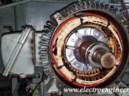
toroidal transformer
Toroidal transformers, in comparison with transformers on armored cores made of Ш-shaped plates, have several advantages:
- smaller volume and weight;
- higher efficiency;
- best cooling for windings.
The primary winding already contained approximately 800 turns of 0.8 mm PELSHO wire, it was filled with paraffin and insulated with a layer of thin PTFE tape.
By measuring the approximate dimensions of the iron of the transformer, you can calculate its overall power, so you can figure out whether the core is suitable for obtaining the required power or not.

Rice. 1. Dimensions of the iron core for a toroidal transformer.
- Overall power (W) \u003d Window area (cm 2) * Cross-sectional area (cm 2)
- Window area = 3.14 * (d/2) 2
- Cross-sectional area \u003d h * ((D-d) / 2)
For example, let's calculate a transformer with iron dimensions: D=14cm, d=5cm, h=5cm.
- Window area \u003d 3.14 * (5cm / 2) * (5cm / 2) \u003d 19.625 cm 2
- Sectional area \u003d 5cm * ((14cm-5cm) / 2) \u003d 22.5 cm 2
- Overall power = 19.625 * 22.5 = 441 watts.
The overall power of the transformer I used turned out to be clearly less than I expected - somewhere around 250 watts.
Selection of voltages for secondary windings
Knowing the required voltage at the output of the rectifier after the electrolytic capacitors, it is possible to approximately calculate the required voltage at the output of the secondary winding of the transformer.
The numerical value of the direct voltage after the diode bridge and smoothing capacitors will increase by about 1.3..1.4 times, compared with the alternating voltage supplied to the input of such a rectifier.
In my case, to power the UMZCH, you need a bipolar constant voltage - 35 volts on each arm. Accordingly, an alternating voltage must be present on each secondary winding: 35 Volts / 1.4 \u003d ~ 25 Volts.
By the same principle, I made an approximate calculation of the voltage values \u200b\u200bfor other secondary windings of the transformer.
Calculation of the number of turns and winding
To power the remaining electronic components of the amplifier, it was decided to wind several separate secondary windings. A wooden shuttle was made for winding coils with copper enameled wire. It can also be made from fiberglass or plastic.
Rice. 2. Shuttle for winding a toroidal transformer.
The winding was carried out with copper enameled wire, which was available:
- for 4 UMZCH power windings - a wire with a diameter of 1.5 mm;
- for other windings - 0.6 mm.
I selected the number of turns for the secondary windings experimentally, since I did not know exact amount turns of the primary winding.
The essence of the method:
- We wind 20 turns of any wire;
- We connect the primary winding of the transformer to the network ~ 220V and measure the voltage on the wound 20 turns;
- We divide the required voltage by that obtained from 20 turns - we find out how many times 20 turns are needed for winding.
For example: we need 25V, and out of 20 turns we get 5V, 25V / 5V = 5 - we need to wind 20 turns 5 times, that is, 100 turns.
Length calculation required wire was done like this: wound 20 turns of wire, made a mark on it with a marker, unwound and measured its length. I divided the required number of turns by 20, multiplied the resulting value by the length of 20 turns of wire - I got approximately the required length of wire for winding. By adding 1-2 meters of stock to the total length, you can wind the wire on the shuttle and safely cut it off.
For example: you need 100 turns of wire, the length of 20 wound turns turned out to be 1.3 meters, we find out how many times 1.3 meters need to be wound to get 100 turns - 100/20=5, we find out the total length of the wire (5 pieces of 1, 3m) - 1.3*5=6.5m. We add 1.5m for the stock and get the length - 8m.
For each subsequent winding, the measurement should be repeated, since with each new winding the length of wire required per turn will increase.
To wind each pair of windings of 25 volts, two wires were laid in parallel on the shuttle at once (for 2 windings). After winding, the end of the first winding is connected to the beginning of the second - we got two secondary windings for a bipolar rectifier with a connection in the middle.
After winding each of the pairs of secondary windings to power the UMZCH circuits, they were insulated with a thin fluoroplastic tape.
Thus, 6 secondary windings were wound: four for powering the UMZCH and two more for power supplies for the rest of the electronics.
Scheme of rectifiers and voltage stabilizers
Below is a schematic diagram of the power supply for my homemade power amplifier.

Rice. 2. Schematic diagram of the power supply for a homemade bass power amplifier.
To power the low-frequency power amplifier circuits, two bipolar rectifiers are used - A1.1 and A1.2. The remaining electronic components of the amplifier will be powered by voltage stabilizers A2.1 and A2.2.
Resistors R1 and R2 are needed to discharge electrolytic capacitors when the power lines are disconnected from the power amplifier circuits.
There are 4 amplification channels in my UMZCH, they can be turned on and off in pairs using switches that switch the power lines of the UMZCH scarf using electromagnetic relays.
Resistors R1 and R2 can be excluded from the circuit if the power supply is constantly connected to the UMZCH boards, in which case the electrolytic capacities will be discharged through the UMZCH circuit.
Diodes KD213 are designed for a maximum forward current of 10A, in my case this is enough. The diode bridge D5 is designed for a current of at least 2-3A, it was assembled from 4 diodes. C5 and C6 are capacitances, each of which consists of two 10,000 microfarad capacitors at 63V.

Rice. 3. Schematic diagrams of DC voltage stabilizers on L7805, L7812, LM317 microcircuits.
Deciphering the names on the diagram:
- STAB - voltage regulator without adjustment, current not more than 1A;
- STAB+REG - adjustable voltage regulator, current not more than 1A;
- STAB+POW - adjustable voltage stabilizer, current approximately 2-3A.
When using LM317, 7805 and 7812 microcircuits, the output voltage of the stabilizer can be calculated using a simplified formula:
Uout = Vxx * (1 + R2/R1)
Vxx for chips has the following meanings:
- LM317 - 1.25;
- 7805 - 5;
- 7812 - 12.
Calculation example for LM317: R1=240R, R2=1200R, Uout = 1.25*(1+1200/240) = 7.5V.
Design
Here's how it was planned to use the voltage from the power supply:
- +36V, -36V - power amplifiers on TDA7250
- 12V - electronic regulators volumes, stereo processors, output power indicators, thermal control circuits, fans, backlight;
- 5V - temperature indicators, microcontroller, digital control panel.
The voltage regulator chips and transistors were mounted on small heatsinks that I removed from non-working computer power supplies. The cases were attached to the radiators through insulating gaskets.
The printed circuit board was made of two parts, each of which contains a bipolar rectifier for the UMZCH circuit and the required set of voltage stabilizers.

Rice. 4. One half of the power supply board.

Rice. 5. The other half of the power supply board.
![]()
Rice. 6. Ready-made power supply components for a homemade power amplifier.
Later, during debugging, I came to the conclusion that it would be much more convenient to make voltage stabilizers on separate boards. Nevertheless, the "all on one board" option is also not bad and convenient in its own way.
Also, a rectifier for UMZCH (diagram in Figure 2) can be assembled by surface mounting, and stabilizer circuits (Figure 3) in the required quantity - on separate printed circuit boards.
The connection of the electronic components of the rectifier is shown in Figure 7.

Rice. 7. Connection diagram for assembling a bipolar rectifier -36V + 36V using surface mounting.
Connections must be made using thick insulated copper conductors.
The diode bridge with 1000pF capacitors can be placed separately on the heatsink. Mounting of powerful KD213 diodes (pills) on one common radiator must be carried out through insulating thermal pads (thermo rubber or mica), since one of the diode leads has contact with its metal lining!
For the filtering circuit (electrolytic capacitors of 10000uF, resistors and ceramic capacitors of 0.1-0.33uF), you can use hastily assemble a small panel - a printed circuit board (Figure 8).

Rice. 8. An example of a panel with slots made of fiberglass for mounting rectifier smoothing filters.
To make such a panel, you need a rectangular piece of fiberglass. Using a homemade cutter (Figure 9), made from a hacksaw blade for metal, we cut the copper foil along the entire length, then we cut one of the resulting parts perpendicularly in half.

Rice. 9. Homemade cutter from a hacksaw blade, made on a grinder.
After that, we outline and drill holes for parts and fasteners, clean the copper surface with thin sandpaper and tin it with flux and solder. We solder the parts and connect to the circuit.
Conclusion
Here is such an uncomplicated power supply was made for a future homemade power amplifier audio frequency. It remains to supplement it with a soft start circuit ( soft start) and standby mode.
UPD: Yuri Glushnev sent a printed circuit board for assembling two stabilizers with voltages + 22V and + 12V. It contains two STAB + POW circuits (Fig. 3) on LM317, 7812 microcircuits and TIP42 transistors.

Rice. 10. Printed circuit board of voltage stabilizers for + 22V and + 12V.
Download - (63 KB).
Another PCB designed for the STAB + REG adjustable voltage regulator circuit based on the LM317:

Rice. 11. Printed circuit board for an adjustable voltage regulator based on the LM317 chip.
Scheme soft start provides a delay of about 2 seconds, which allows you to smoothly charge larger capacitors without power surges and blinking light bulbs at home. The charge current is limited by the value: I=220/R5+R6+Rt.
where Rt is the resistance of the primary winding of the transformer direct current, Om.
The resistance of resistors R5, R6 can be taken from 15 ohms to 33 ohms. Less - not effective, but more - the heating of the resistors increases. With the ratings indicated on the diagram, the maximum starting current will be limited, approximately: I=220/44+(3...8)=4.2...4.2A.
The main questions that beginners have when assembling:
1. What voltage should electrolytes be set to?
Electrolyte voltage is indicated on printed circuit board are 16 and 25V.
2. What voltage should a non-polar capacitor be set to?
Its voltage is also indicated on the printed circuit board - it is 630V (400V is allowed).
3. What transistors can be used instead of BD875?
KT972 with any letter index or BDX53.
4. Can a non-composite transistor be used instead of the BD875?
It is possible, but it is better to look for a composite transistor.
5. Which relay should be used?
The relay must have a 12V coil with a current of no more than 40mA, and preferably 30mA. Contacts must be rated for a current of at least 5A.
6. How to increase the delay time?
To do this, it is necessary to increase the capacitance of the capacitor C3.
7. Is it possible to use a relay with a different coil voltage, for example 24V?
No, the circuit won't work.
8. Collected - does not work
So this is your mistake. The circuit assembled on serviceable parts starts working immediately and does not require adjustment and selection of elements.
9. There is a fuse on the board, what current should it be used for?
I recommend calculating the fuse current as follows: Ip \u003d (Pbp / 220) * 1.5. The resulting value is rounded up to the nearest fuse rating.

Discussion of the article on the forum:
List of radio elements
| Designation | A type | Denomination | Quantity | Note | Score | My notepad |
|---|---|---|---|---|---|---|
| VT1 | bipolar transistor | BDX53 | 1 | KT972, BD875 | To notepad | |
| VDS1 | rectifier diode | 1N4007 | 4 | To notepad | ||
| VD1 | zener diode | 1N5359B | 1 | 24 V | To notepad | |
| VD2 | rectifier diode | 1N4148 | 1 | To notepad | ||
| C1 | Capacitor | 470 nF | 1 | At least 400 V | To notepad | |
| C2, C3 | electrolytic capacitor | 220uF | 2 | 25 V | To notepad | |
| R1 | Resistor | 82 kOhm | 1 | To notepad | ||
| R2 | Resistor | 220 ohm | 1 | 2 W | To notepad | |
| R3 | Resistor | 62 kOhm | 1 | To notepad | ||
| R4 | Resistor | 6.8 kOhm | 1 | To notepad | ||
| R5, R6 | Resistor |
Scheme of soft power-on (soft start or stepped power-up) for a low-frequency power amplifier or other device. This simple device improves the reliability of your radio and reduces network interference when you turn it on.
circuit diagram
Any radio power supply contains rectifier diodes and high-capacity capacitors. At the initial moment of turning on the mains supply, a pulsed current surge occurs - while the filter capacitances are being charged.
The amplitude of the current pulse depends on the value of the capacitance and the voltage at the output of the rectifier. So, at a voltage of 45 V and a capacitance of 10,000 microfarads, the charging current of such a capacitor can be 12 A. In this case, the transformer and rectifier diodes briefly operate in short circuit mode.
To eliminate the risk of failure of these elements by reducing the inrush current at the time of initial switching on, the circuit shown in Figure 1 is used. It also allows you to lighten the modes and other elements in the amplifier for the duration of the transients.
Rice. 1. Schematic diagram of the smooth switching on of the power source using a relay.
At the initial moment, when power is applied, capacitors C2 and C3 will be charged through resistors R2 and R3 - they limit the current to a safe value for the rectifier parts.
After 1 ... 2 seconds, after the capacitor C1 is charged and the voltage on the relay K1 increases to a value at which it will operate and with its contacts K1.1 and K1.2 shunt the limiting resistors R2, R3.
In the device, you can use any relay with a response voltage less than that acting at the output of the rectifier, and the resistor R1 is selected so that the "excess" voltage drops across it. The relay contacts must be rated for the maximum current in the power supply circuits of the amplifier.
The circuit uses a relay RES47 RF4.500.407-00 (RF4.500.407-07 or others) with a rated operating voltage of 27 V (winding resistance 650 Ohm; current switched by contacts can be up to 3 A). In fact, the relay is already activated at 16 ... 17 V, and the resistor R1 is selected with a value of 1 kOhm, while the voltage across the relay will be 19 ... 20 V.
Capacitor C1 type K50-29-25V or K50-35-25V. Resistors R1 type MLT-2, R2 and R3 type C5-35V-10 (PEV-10) or similar. The value of the resistors R2, R3 depends on the load current, and their resistance can be significantly reduced.
Improved Device Schematic
The second scheme shown in fig. 2 performs the same task, but reduces the size of the device by using a smaller time-setting capacitor C1.
Transistor VT1 turns on relay K1 with a delay after capacitor C1 is charged (type K53-1A). The circuit also allows, instead of switching the secondary circuits, to provide a stepped voltage supply to the primary winding. In this case, you can use a relay with only one group of contacts.

Rice. 2. Improved circuit diagram for smooth switching on the UMZCH power supply.
The resistance value R1 (PEV-25) depends on the load power and is chosen such that the voltage in the secondary winding of the transformer is 70 percent of the nominal value with the resistor on (47 ... 300 Ohm). Setting up the circuit consists in setting the delay time for turning on the relay by selecting the value of the resistor R2, as well as choosing R1.
In conclusion
The above schemes can be used in the manufacture of a new amplifier or in the modernization of existing ones, including industrial ones.
Compared to similar devices for two-stage supply voltage supply, given in various magazines, those described here are the simplest.
Primitive: unknown.
THE ARTICLE IS PREPARED ON THE BASIS OF THE BOOK BY A. V. GOLOVKOV and V. B LYUBITSKY "POWER SUPPLIES FOR SYSTEM MODULES OF THE TYPE IBM PC-XT/AT" PUBLISHING HOUSE "LAD i N"
"SLOW START" SCHEME
When turned on impulse block power supply, the output filter capacitors are not yet charged. Therefore, the transistor converter actually operates on a short-circuited load. In this case, the instantaneous power at the collector junctions of high-power transistors can exceed several times the average power consumed from the network. This is because the feedback action at start-up causes the transistors to over-current. Therefore, measures are needed to ensure a "smooth" ("soft" or "slow") start of the converter. In the UPSs under consideration, this is achieved by smoothly increasing the duration of the on state of powerful transistors, regardless of the feedback signal, which “requires” the control circuit for the maximum possible duration of the control pulse immediately when the UPS is turned on. Those. the fill factor of the impulse voltage at the moment of switching on is forcibly made very small and then gradually increases to the required value. "Slow start" allows the control chip IC1 to gradually increase the duration of the pulses on pins 8 and 11 until the PSU reaches the nominal mode. In all UPSs based on the control IC type TL494CN, the "slow start" circuit is implemented using an RC circuit connected to the non-inverting input of the "dead zone" comparator DA1 (pin 4 of the microcircuit). Consider the operation of the start-up circuit using the LPS-02-150XT UPS as an example (Fig. 41). "Slow start" is carried out in this circuit thanks to the RC chain C19, R20 connected to pin 4 of the control chip IC1.
Before considering the operation of the "soft start" scheme, it is necessary to introduce the concept of the UPS startup algorithm. The startup algorithm refers to the sequence in which voltages appear in the UPS circuit. In accordance with the physics of work, the rectified mains voltage Uep always appears initially. Then, as a result of the triggering circuit, the supply voltage of the Upom control chip appears. The result of applying power to the microcircuit is the appearance of the output voltage of the internal stabilized reference voltage source Uref. Only after that the output voltages of the block appear. The sequence of appearance of these voltages cannot be broken, i.e. Uref, for example, cannot appear before Upom, etc.
Note Please pay special attention to the fact that the process of the initial start-up of the UPS and the process of "slow start" are different processes that occur sequentially in time! When the UPS is connected to the network, the initial start-up occurs first, and only then - a "slow start", which makes it easier for the power transistors of the unit to enter the nominal mode.
As already noted, the ultimate goal of the "slow start" process is to obtain output control pulses that gradually increase in width at pins 8 and 11. The width of the output pulses is determined by the width of the output pulses logic element DD1 IC1 (see fig. 13). The flow of the UPS soft start process in time is shown in fig. 47.
Let the control chip IC1 be supplied with the supply voltage Upom at time t0. As a result, the sawtooth voltage generator DA6 is started, and the reference voltage Uref appears at pin 14. The sawtooth output voltage of the generator is supplied to the inverting inputs of comparators DA1 and DA2. The output voltage of the error amplifier DA3 is applied to the inverting input of the PWM comparator DA2. Since the output voltages of the unit (including + 5V) are still absent, the feedback signal taken from the divider R19, R20 and applied to the non-inverting input of the error amplifier is 0. A certain positive voltage is applied to the inverting input of this amplifier, taken from divider SVR, R24, R22 in the reference voltage bus circuit Uref, which is already available. Therefore, the output voltage of the error amplifier DA3 will be equal to 0 at the initial moment, and as the output capacitors of the filters charge, it will increase. The output voltage of the PWM comparator DA2 for this reason will be a pulse train that grows in width. This process is shown in time diagrams 1 and 2 (Fig. 47).
Figure 47. Timing diagrams explaining the process of a smooth (soft) start of the UPS and illustrating the operation of the control HMCTL494 in starting mode: U3, U4, U5 - voltages at the IC pins 3, 4 and 5, respectively.
The non-inverting input of the dead zone comparator DA1 is connected to pin 4 of IC1. An external RC circuit C19, R20 is connected to this output, which is powered from the reference voltage bus Uref. Therefore, when Uref appears, all of it is allocated at the first moment on the resistor R20, because capacitor C19 is completely discharged. As C19 charges, the current through it and resistor R20 decreases. Therefore, the voltage drop across R20, which is applied to pin 4 1C 1, has the form of a falling exponential. In accordance with this, the output voltage of the "dead zone" comparator DA1 will be a sequence of pulses decreasing in width. This process is shown in time diagrams 3 and 4 (Fig. 47). Thus the processes of latitudinal change output voltages comparators DA1 and DA2 are mutually opposite.
The output voltages of the comparators are input to the logic element DD1 (2-OR). Therefore, the pulse width at the output of this element is determined by the widest of the input pulses.
From the timing diagram 5 (Fig. 47), which displays the output voltage of DD1, it can be seen that, up to the moment ti, the width of the output pulses of the comparator DA1 exceeds the width of the output pulses of the PWM comparator DA2. Therefore, the switching of this comparator does not affect the width of the output pulse DD1, and hence the output pulse IC1. The determining factor in the interval to-t-i is the output voltage of the comparator DA1. The width of the output pulses of IC1 gradually increases in this interval, as can be seen from the timing diagrams 6 and 7 (Fig. 47).
At the moment ti, the output pulse of the comparator DA1 is compared in width with the output pulse of the PWM comparator DA2. At this moment, control is transferred from the comparator DA1 to the PWM comparator DA2, because. its output pulses begin to exceed the width of the output pulses of the comparator DA1. During the time t0-t, the output capacitors of the filters have time to charge smoothly, and the unit has time to enter the nominal mode.
Thus, the essence of the circuitry solution to the problem of "soft" start is that during the charging of the capacitors of the output filters, the PWM comparator DA2 is replaced by the comparator DA1, whose operation does not depend on the feedback signal, but is determined by a special forming RC circuit C19.R20.
From the material discussed above, it follows that before each switching on of the UPS, the capacitor of the forming RC circuit (in this case, C19) must be completely discharged, otherwise a "soft" start will not be possible, which can lead to failure of the power transistors of the converter. Therefore, in each UPS circuit, a special circuit is provided to quickly discharge the capacitor of the forming circuit when the UPS is turned off from the mains or when the current protection is triggered.
PG (POWER GOOD) SIGNAL PRODUCTION CIRCUITS
PG signal, along with four output supply voltages system block, is the standard output parameter of the UPS.
The presence of this signal is mandatory for any block that complies with the IBM standard (not just blocks built on the basis of the TL494 chip). However, XT-class computers sometimes do not use this signal.
The UPS has a wide variety of PG signal generation schemes. Conventionally, the whole variety of schemes can be divided into two groups: one non-functional and two-functional.
Some non-functional circuits implement only the function of delaying the appearance of the H-level PG signal allowing the processor to start when the UPS is turned on.
Dual-functional circuits, in addition to the above function, also implement the function of pre-emptively transitioning the PG signal to an inactive low level, which prohibits the operation of the processor when the UPS is turned off, as well as in cases of various kinds of emergencies, before the supply digital part begins to decrease system module voltage +5V.
Most PG signal generation circuits are dual function, but they are more complex than the first type circuits.

Figure 48. Functional diagram IC LM339 (top view).

Figure 49. Principal circuit diagram one comparator IC LM339.

Figure 50. PG signal formation diagram in UPS GT-200W
As base element in the construction of these circuits, a microcircuit of the LM339N type is widely used, which is a quad voltage comparator (Fig. 48).
The output transistors of each comparator have an open collector (Fig. 49). Pin 12 of the LM339N is connected to the "case", and pin 3 is supplied with unipolar (from + 2V to + ZOV) power.
Due to the high sensitivity of the comparator circuits, the required speed is provided.
Let us consider in more detail several characteristic options for constructing circuits for generating a PG signal.
The PG signal generation circuit used in the GT-200W is shown in fig. 50.
When the unit is connected to the network, the start circuit is triggered and a reference voltage of +5.1V appears on the Uref bus from the internal source of the TL494 chip. There is no +5V output yet. Therefore, the feedback divider R25, R24 is not yet powered (the potential of output 1 of the microcircuit is 0V). The divider, which gives the reference level at pin 2 of the microcircuit, is already powered by the voltage Uref. Therefore, the output voltage of the error amplifier is minimal (at pin 3, the potential is about 0V), and the transistor Q7, fed through the collector with the same voltage Uref, is open and saturated with the base current flowing through the circuit: Uref - R36 - e-6 Q7 - R31 - internal circuits TL494 - "frame".
The potential of the non-inverting input of comparator 1 of IC2 (LM339N) is 0, and since at its inverting input there is a positive potential from the resistor R42 of the divider R35, R42 in the Uref circuit, the comparator itself will be in the 0V state at the output (the output transistor of the comparator is open and saturated). Therefore, the PG signal has an L-level and disables the processor.
Next, the +5V output voltage begins to appear as the high-capacity output capacitors charge. Therefore, the output voltage of the error amplifier DA3 begins to increase, and the transistor Q7 closes. As a result, the retaining capacitance C16 begins to become infected. The charging current flows through the circuit: Uref -R36- C16- "case".
As soon as the voltage at C16 and at the non-inverting input of comparator 1 (pin 7 of IC2) reaches the reference level at its inverting input (pin 6 of IC2), the output transistor of the comparator will turn off. PIC, which covers the comparator 1 (resistor R34), causes the presence of hysteresis on the transfer characteristic of this comparator. This ensures the reliability of the operation of the PG circuit and eliminates the possibility of the comparator "tipping" under the influence of random impulse interference (noise). By this time, the full nominal voltage appears on the + 5V bus, and the PG signal becomes an H-level signal.
From the foregoing, it can be seen that the block status sensor (on / off) in this circuit is the output voltage of the error amplifier DA3, taken from pin 3 of the control chip IC1 (TL494), and the circuit is single-functional.
More complex scheme PG signal generation is implemented in the APPIS UPS (Fig. 51).

Figure 51. Scheme of PG signal formation in the Appis UPS.
This circuit uses three comparators on IC2.
The power-on delay function is implemented as follows.
After the UPS is connected to the network and the start circuit is triggered, the reference voltage Uref appears. The output voltages of the unit are not yet available. Therefore, IC2 and Q3 are not yet powered. Transistor Q4, from the collector of which the PG signal is taken, is open, because. write down its base divisor. The base current flows through the circuit: Uref-R34 - R35 -6-3Q4- "case".
Therefore, PG has an L-level. In addition, the capacitor C21 is charged from the Uref bus along the circuit: Uref-R29-C21 - "body".
With the advent of the block output voltages from the + 12V bus, the IC2 chip and the Q3 transistor are powered through the decoupling filter R38, C24. From the + 5V bus, transistor Q4 is fed through the collector with full voltage. In this case, the following processes take place.
Starting from the moment the unit is turned on, the inverting input of the controlling comparator receives an unsmoothed voltage rectified by a two-half-wave circuit D5, D6 from the secondary winding 3-4-5 of a special transformer T1. This pulsating voltage with an amplitude of about 15V is supplied to the inverting input of comparator 2 through the amplitude limiting link R24, ZD1 (11V zener diode) and the resistive divider R25, R26. Since the amplitude of the pulses after limiting and dividing still remains greater than the level of the reference voltage at the non-inverting input of comparator 2, then with each pulse and for almost the entire duration of its operation, comparator 2 is transferred to the 0V state at the output (the output transistor of the comparator will be open). Therefore, in a few pulses, the delay capacitor C21 is discharged to almost 0V. Therefore, comparator 1 switches to the 0V state at the output, since the voltage at its non-inverting input is determined by the voltage level across the capacitor C21. As a result, transistor Q3 is locked to zero bias. Locking Q3 leads to the charging of the second delay capacitor C23 along the circuit: + 12V - R38 - R32 - R33 - C23 - "case".
As soon as the voltage at the Q3 collector, and therefore at the inverting input of comparator 3, reaches the threshold level at its inverting input (Uref=+5.1V), comparator 3 switches to 0V at the output (the output transistor of the comparator opens). Therefore, the base divider for Q4 R35, R36 will be unpowered, and Q4 will be disabled.
Since there is already full voltage on the +5V rail, and Q4 is turned off, the PG signal becomes H-level.
The power off lookahead function is implemented as follows.
When the unit is turned off from the network, the rectified voltage immediately ceases to flow from the secondary winding 3-4-5 TL and the rectification circuits D5, D6. Therefore, comparator 2 immediately switches, its output transistor closes. Next, it starts charging from Uref through R29 delay capacitance C21. This prevents the circuit from tripping during random short-term dips. mains voltage. When C21 is charged to half the voltage Uref, comparator 1 will switch. Its output transistor will turn off. Then transistor Q3 will open with the base current flowing through the circuit: +726 - R38 - R31 -D21-6-9Q3- "case".
The capacity of the second delay C23 is quickly discharged through Q3 and the accelerating diode D20 along the circuit: (+) C23 - D20 - to-e Q3 - "case" - (-) C23.
The potential of the inverting input of comparator 3 will rapidly decrease with the discharge rate of C23. Therefore, comparator 3 switches, its output transistor closes, and the base divider for Q4 is powered from the Uref bus. Therefore, Q4 will open to saturation, and the PG signal will become L-level, warning the digital part of the system unit about the upcoming loss of supply voltages.
Thus, in this circuit, the block state sensor (on/off) is the presence or absence of a transformed mains voltage (through transformer T1), and the circuit is two-functional.
The KYP-150W power supply uses a PG signal generation circuit using two comparators of the LM339N chip (Fig. 52).

Rice. Fig. 52. PG signal formation diagram in KYP-150W UPS (TUV ESSEN FAR EAST CORP.).
In this scheme, the block status sensor is the level of the auxiliary supply voltage Upom of the TL494 chip.
The scheme works as follows. When the UPS is connected to the network, the start-up circuit is activated, as a result of which voltage appears on the Upon bus, which powers the TL494 control chip. As soon as Upom reaches a level of about + 7V, the microcircuit starts up and the output voltage of the internal reference source Uref = + 5V appears at pin 14 of it. The output voltages of the unit are not yet available. IC2 (LM339N) is powered by Uref at pin 3.
When Upom reaches a level of about + 12V, the zener diode ZD1 "breaks through", and a voltage drop appears on the resistor R34, which increases with the growth of Upom. When the drop across R34 reaches the level of the reference voltage across the resistor R48 of the divider R51, R48 in the Uref circuit, comparator 2 of IC2 will be set to the H-level output state (its output transistor will close). Therefore, the diode D22 will be locked. The charge of the delay capacitance C15 begins along the chain: Uref- R49- C15- "body"
This process introduces a delay for comparator 1 of IC2 to "roll over" and the H-level enable signal PG to appear. During this time, the "soft" start process has time to occur, and the output voltages of the unit appear in full, i.e. the unit reliably enters the nominal mode. As soon as the voltage at C15 reaches the reference level across resistor R48, comparator 1 will "tip". Its output transistor will turn on, and therefore transistor Q7 will be locked to zero bias. The PG signal taken from the collector load Q7 will become H-level, which will allow the system module processor to start.
When the unit is turned off from the network, the Upom voltage begins to disappear first, because. storage capacitors that maintain the voltage on the Uporn bus have a small capacitance. As soon as the voltage drop across resistor R34 drops below the reference level across resistor R48, comparator 2 of IC2 will switch. Its output transistor will open, and through it and the diode D22, the delay capacitance C15 will quickly discharge. The discharge occurs almost instantly, because. there is no limiting resistance in the discharge current flow circuit. Immediately after this, comparator 1 of IC2 will also switch. PIC through diode D21, covering comparator 1, causes the presence of hysteresis in the transient response of the comparator. The output transistor of the comparator will close and the base current flowing through the circuit: Uref - R50 - 6-e Q7 - "case", transistor Q7 will open. The PG signal will become L-level, warning of the upcoming loss of the unit's output voltages. In this way, this scheme is bifunctional.
The GT-150W UPS uses a PG signal generation circuit that only implements the turn-on delay function (Fig. 53).

Figure 53. PG signal formation diagram in UPS GT-150W
After turning on the IVP and triggering the start circuit, voltages begin to appear on the output buses of the unit. Capacitor C23 begins to charge along the circuit: bus +56 - C23 - R50 - 6-e Q7- "body".
This current opens transistor Q7 to saturation, from the collector of which the signal PG is removed. Therefore, the PG signal will be L-level for almost the entire time C23 is being charged. As soon as the voltage on the + 5V bus stops increasing, having reached the nominal level, the charging current C23 stops flowing. Therefore, Q7 will close and the PG signal will become an H-level signal.
Diode D16 is needed to quickly and reliably discharge C23 after turning off the UPS.
Thus, PG signal generation schemes can be classified according to the physical principle underlying their construction:
circuits built on the basis of monitoring the output voltage of the internal voltage error amplifier DA3 of the control microcircuit or (which is the same) controlling the level of the feedback signal from the +5V output voltage bus;
circuits built on the basis of level control and the presence of an alternating mains voltage at the input of the unit;
circuits built on the basis of controlling the level of the auxiliary supply voltage of the Upom control chip.
circuits built on the basis of monitoring the presence of a pulsed alternating high-frequency voltage on the secondary side of a power pulse transformer.
Consider one of the options for implementing the last type of circuit, which is used, for example, in the HPR-200 UPS circuit (Fig. 54). The construction of this circuit is based on the idea of controlling the presence of an alternating pulsed voltage on the secondary winding of the power pulse transformer T1. The scheme works as follows.

Figure 54. PG signal generation diagram in HPR-200 UPS (HIGH POWER ELECTRONIC Co., Ltd)
When the UPS is connected to the network, the smoothing capacitors of the output voltage bus + 5V C4, C5 of large capacity (2x33Omkf) are completely discharged. The capacitors C1, C2, C3 are also discharged. The pulse alternating voltage that appears on the secondary winding 3-5 of the power pulse transformer T1 begins to charge the capacitors C4, C5. A half-wave rectifier D1 is connected to tap 5 of the secondary winding. C1 - smoothing capacitance of the filter. R1 (10 Ohm) - current limiting resistor. Capacitor C1 of small capacity (150nF) is charged to a level of about + 10V almost immediately (with the first pulse).
As soon as the +5V bus potential level exceeds the minimum allowable supply voltage for IC1 (+2V), the microcircuit will start to function. The voltage from the capacitor C1 is supplied to the resistive divider R2, R3. Part of this voltage is removed from R3 and fed to the non-inverting input of comparator A (pin 9 of IC1), as well as to the divider R4, R6, C2. Therefore, in parallel with the growth of the bus potential + 5V, the capacitor C2 is charged along the circuit: (+) C1 - R2 - R4 - C2 - "case" - (-) C1.
By the time the +5V rail potential reaches IC1's minimum power supply (+2V), this capacitor will be charged. Therefore, the comparators of the microcircuit are set to the following state:
comparator A - the output transistor is closed, because the potential of the non-inverting input is higher than the potential at the inverting input;
comparator B - the output transistor is open, because the potential of the non-inverting input is lower than the potential of the inverting input.
This distribution of potentials is due to the values of the resistors connected to the inputs of the comparators.
The PG signal, taken from the collector load R11 of the output transistor of comparator B, is 0V and prohibits the processor from starting. Meanwhile, the process of recharging the storage capacitors C4, C5 is underway and the + 5V bus potential is growing. Therefore, the charge current of the capacitor SZ flows through the circuit: bus +56 - R9 - R8 - SZ - "body".
The voltage across the capacitor C3, and hence at the non-inverting input of comparator B, is growing. This increase occurs until the potential of the non-inverting input of comparator B begins to exceed the potential of its inverting input. As soon as this happens, comparator B switches, its output transistor closes. The voltage on the + 5V bus reaches the nominal level by this moment. Therefore, the PG signal becomes the signal high level and allows the processor to start. Thus, the capacitance of the capacitor C3 causes a delay in turning on.
When you turn off the switching power supply from the network, the alternating impulse voltage disappears on the secondary winding 3-5 T1. Therefore, the small capacitor C1 is quickly discharged, and the voltage at the non-inverting input of comparator A quickly decreases to 0V. The voltage at the inverting input of this comparator drops much more slowly due to the charge on the capacitor C2. Therefore, the potential of the inverting input becomes higher than the potential of the non-inverting input, and comparator A switches. Its output transistor opens. Therefore, the potential of the non-inverting input of comparator B becomes 0V. The potential of the inverting input of comparator B is still positive due to the charge on the capacitor C2. Therefore, comparator B switches, its output transistor opens, and the PG signal goes low, initializing the system reset signal RESET, before the +5 V supply voltage to the logic chips decreases below the acceptable level.
Comparators A and B are positively-feedbacked by resistors R7 and R10, respectively, which speeds up their switching.
Precision resistive divider R5, R6 sets the reference voltage level at the inverting inputs of comparators A and B in the nominal operating mode.
Capacitor C2 is required to maintain this reference level after the UPS has been switched off from the mains.
In conclusion of this section, we present one more variant of the implementation of the PG signal generation scheme (Fig. 55).

Figure 55. Diagram of PG signal formation in UPS SP-200W.
The scheme is single-functional, i.e. implements only the delay in the appearance of the enable signal PG when the TRS is connected to the network.
In this circuit, the controlled signal is the voltage level on the +12V channel output bus. The circuit design is based on a two-stage UPT circuit on transistors Q10, Q11, covered by positive feedback using resistor R55. The rollover delay of this circuit is due to the presence of a relatively large capacitor C31 in the base circuit of the Q10 FET. After turning on the UPS in the network, while the process of entering the mode is in progress, the charging current of the capacitor C31 flows from the output bus of the + 12V channel through the circuit: bus + 12V -R40-C31 - "case".
The voltage across the capacitor C31 gradually increases. As long as this voltage does not reach the trip threshold level of the circuit on transistors Q10, Q11, this circuit is in a state in which the transistor Q10 is closed, and the transistor Q11 is open by the base current that flows from the output rail of the +5V channel under the influence of a growing voltage on the capacitors of this rail : tire +56 - R41 - 6th Q11 - "case".
Therefore, the PG signal taken from the collector of Q11 is 0V, and prohibits the processor from starting. Meanwhile, a rising voltage across capacitor C31 is applied to the base divider R43, R44 of transistor Q10. By the time the UPS output voltages reach the nominal levels, the voltage at C31 will reach a level sufficient for the occurrence of an avalanche process of mutual change in the states of transistors Q10, Q11 (due to the presence of POS). As a result, transistor Q10 will be open to saturation, and transistor Q11 will be closed. Therefore, the PG signal will become a high level signal and the processor will be allowed to start. Diode D20 is used to quickly discharge the capacitor C31 after the UPS is turned off from the network. In this case, C31 is discharged through diode D20 and a discharge resistor of the + 5V channel output bus (not shown in the diagram). In addition, during the operation of the UPS, this diode limits the voltage level on the capacitor C31. The limit level is about +5.8V.
In addition to the above PG signal generation schemes, other principles for constructing circuits can be used, and a different number of comparators of the LM339N chip can be used - from one to four.
| MAIN PARAMETERS OF SWITCH POWER SUPPLY FOR IBM | The main parameters of switching power supplies are considered, the pinout of the connector is given, the principle of operation from a mains voltage of 110 and 220 volts, | |
| The TL494 microcircuit, the switching circuit and the use cases for controlling the power switches of switching power supplies are described in detail. | ||
| CONTROL OF THE POWER KEYS OF THE SLEEPING POWER SUPPLY WITH THE HELP OF TL494 | The main methods of controlling the basic circuits of power transistors of switching power supplies, options for constructing secondary power rectifiers are described. | |
| STABILIZATION OF OUTPUT VOLTAGES OF PULSE POWER SUPPLY | The options for using error amplifiers TL494 for stabilizing output voltages are described, the principle of operation of the group stabilization choke is described. | |
| PROTECTION SCHEMES | Several options for constructing systems for protecting impulse power supplies from overload are described. | |
| "SLOW START" SCHEME | The principles of soft start formation and POWER GOOD voltage generation are described. | |
| EXAMPLE OF CONSTRUCTION OF ONE OF THE PULSED POWER SUPPLY | Full description circuit diagram and its operation of a switching power supply | |
One of the most important problems that arise in the design of radio equipment is the problem of ensuring its reliability. The solution to this problem is based on the optimal calculation of the design of the apparatus and good adjustment during its manufacture. However, even in an optimally designed and adjusted device, there is always a risk of its failure at the moment the mains power is turned on. This danger is greatest for equipment with high power consumption - an audio frequency power amplifier (UMZCH).
The fact is that at the moment the mains power is turned on, the elements of the UMZCH power supply experience significant impulse current overloads. The presence of high-capacity discharged oxide capacitors (up to tens of thousands of microfarads) in rectifier filters causes an almost short circuit of the rectifier output at the time of power-on.
With a supply voltage of 45 V and a filter capacitor capacitance of 10,000 uF, the charging current of such a capacitor at the moment the power is turned on can reach 12 A. Practically at this moment, the power supply transformer operates in short circuit mode. The duration of this process is short, but it is quite sufficient under certain conditions to disable both the power transformer and the rectifier diodes.
In addition to the power supply, the UMZCH itself experiences significant overloads at the time the power is turned on. They are caused by non-stationary processes occurring in it due to the establishment of active element modes in terms of current and voltage and slow inclusion of embedded systems into operation. feedback. And the higher the nominal supply voltage of the UMZCH, the greater the amplitude of such overloads and, accordingly, the higher the likelihood of damage to the amplifier elements.
Of course, earlier attempts were made to protect the UMZCH from overloads when the power was turned on. A device was proposed that protected the amplifier from overloads, made in the form of a powerful bipolar supply voltage stabilizer, which, when turned on, initially applied a voltage of ±10 V to the amplifier, and then gradually increased it to a nominal value of ±32 V. According to the author of this device, it allowed to significantly improve the reliability of the UMZCH and abandon the use of traditional systems protected acoustic systems from overloads at power-up.
With the indisputable advantages of this device, it also has disadvantages - the device protected only the UMZCH, but left its power supply unprotected, due to the complexity of its own design, it was unreliable in itself.
Your attention is invited to a simple and reliable UMZCH “soft” power-on device that protects both the UMZCH itself and its power supply from overloads. It is available for manufacturing even to a novice radio designer and can be used both in the development of new models of radio equipment and in the modernization of existing ones, including industrial production.
Principle of operation
The principle of operation of the device consists in a two-stage supply of supply voltage to the primary winding of the transformer of the UMZCH power supply. A powerful ballast resistor is connected in series to the primary winding circuit of the power supply transformer (Fig. 1). The value of its resistance is calculated in accordance with the overall power of the transformer so that when turned on, the AC voltage on the primary winding is approximately half the mains voltage.
Then, at the moment of switching on, respectively, both the alternating voltage of the secondary windings of the transformer and the supply voltage of the UMZCH will be twice less. Due to this, the amplitudes of the current and voltage pulses on the elements of the rectifier and UMZCH sharply decrease. Non-stationary processes at a reduced supply voltage proceed much "softer".
Then, a few seconds after the power is turned on, the ballast resistor R1 is closed by the contact group K1.1 and the full mains voltage is applied to the primary winding of the power transformer. Accordingly, the power supply voltage is restored to the nominal values.
By this time, the rectifier filter capacitors are already charged to half the nominal voltage, which eliminates the occurrence of powerful current pulses through the secondary windings of the transformer and rectifier diodes. In UMZCH, by this time, non-stationary processes are also completed, feedback systems are turned on, and the supply of full supply voltage does not cause any overloads in UMZCH.
When the mains power is turned off, contacts K1.1 open, the ballast resistor is again connected in series with the primary winding of the transformer, and the whole cycle can be repeated. The soft power-on device itself consists of a transformerless power supply, a timer loaded on an electromagnetic relay. The design of the device and the modes of its elements are selected taking into account the maximum safety margin in operation. Its scheme is shown in fig. one.
When the mains voltage is supplied to the UMZCH power supply by the SB1 switch through the current-limiting elements R2 and C2, it is simultaneously supplied to a bridge rectifier assembled on diodes VD1 - VD4. The rectified voltage is filtered by the capacitor C3, limited by the Zener diode VD5 to a value of 36V and fed to a timer made on the transistor VT1. The current flowing through the resistors R4 and R5 charges the capacitor C4, upon reaching a voltage of approximately 1.5 V on it, the transistor VT1 goes into the open state - the relay K1 is activated and the contacts K1.1 shunt the ballast resistor R1.
Details
The design of the device uses a hermetic electromagnetic relay RENZZ version RF4.510.021 with an operating voltage of 27 V and a trip current of 75 mA. It is also possible to use other types of relays that allow switching an inductive load of alternating current with a frequency of 50 Hz of at least 2 A, for example, REN18, REN19, REN34.
As VT1, a transistor with a large value of the current transfer coefficient parameter - KT972A was used. It is possible to use the transistor KT972B. In the absence of these transistors, transistors with a p-n-p conductivity structure are suitable, for example, KT853A, KT853B, KT973A, KT973B, but only in this case the polarity of all diodes and capacitors this device should be reversed.
In the absence of transistors with a high current transfer coefficient, a composite transistor circuit of two transistors can be used according to the circuit shown in Fig. 2. As VT1 in this circuit, any silicon transistors with a permissible collector-emitter voltage of at least 45 V and a sufficiently high current gain, for example, types KT5OZG, KT3102B, are applicable. As a transistor VT2 - medium power transistors with the same parameters, for example, KT815V, KT815G, KT817V, KT817G or similar. The connection of the composite transistor variant is made in points A-B-C the main circuit of the device.
In addition to diodes KD226D, diodes KD226G, KD105B, KD105G can be used in the device. As a capacitor C2, a capacitor of the MBGO type with an operating voltage of at least 400 V is used. The parameters of the current-limiting circuit R2C2 provide maximum alternating current approximately 145 mA, which is sufficient when an electromagnetic relay with a trip current of 75 mA is used.
For a relay with a trip current of 130 mA (REN29), the capacitance of capacitor C2 will need to be increased to 4 μF. When using a relay type REN34 (operating current 40 mA), a capacitance of 1 μF is sufficient. In all options for changing the capacitance of a capacitor, its operating voltage should be at least 400 V. In addition to metal-paper capacitors, good results can be obtained using metal-film capacitors of types K73-11, K73-17, K73-21, etc.
Vitrified wire resistor PEV-25 is used as a ballast resistor R1. The indicated resistor power rating is calculated for use with a power transformer having an overall power of about 400 watts. For a different value of the overall power and half voltage of the first stage, the resistance of the resistor R1 can be recalculated using the formula:
R1 (Ohm) = 48400 / Slave (W).
Setting
Adjusting the device is reduced to setting the timer to delay the start of the second stage. This can be done by selecting the capacitance of capacitor C5, so it is advisable to make it up of two capacitors, which will facilitate the adjustment process.
Note: In the author's version of the device, there is no fusible link (fuse) in the power circuit. In the nominal mode of operation, it is, of course, not required. But there can always be emergency situations - short circuits, breakdowns of elements, etc. because the author himself argues the need to use his design in just such a situation, then the role of the protective element is taken over by the resistor R2, it warms up and burns out.
The use of a fusible link in emergency situations is quite justified. It's cheaper, easier to get, and the response time is so short that other elements don't have time to heat up and cause any additional damage. And finally, this is a generally accepted, proven method of protecting devices from the possible consequences of equipment malfunctions, worked out many times over.
Literature:
- Sukhov N. UMZCH high fidelity. - Radio, 1989, No. 6, 7.
- Kletsov V. LF amplifier with low distortion. - Radio, 1983, No. 7, p. 51-53; 1984, no. 2, p. 63-64.