Diffusion capacitance of a semiconductor diode relative to the barrier capacitance. Semiconductor diodes, p-n junction, types of breakdowns, barrier capacitance, diffusion capacitance
Reverse flow mechanism through the transition is relatively simple. Charge carriers that are minor for one of the regions, drifting in the electric field of the volume charge region, fall into the region where they are already the main carriers. Since the concentration of majority carriers usually significantly exceeds the concentration of minority carriers in the neighboring region (n n>> np and p p >> p n), then the appearance in a particular region of the semiconductor of an insignificant additional amount of the main charge carriers practically does not change the equilibrium state of the semiconductor.
A different picture is obtained with the flow of direct current . In this case, the diffusion component of the current dominates, consisting of majority charge carriers that overcome the potential barrier and penetrate into the region of the semiconductor, for which they are minority carriers. In this case, the concentration of minority carriers can increase significantly in comparison with the equilibrium concentration. The phenomenon of the introduction of nonequilibrium carriers is called injection.
When direct current flows through p-n- the transition from the electronic region to the hole region will be the injection of electrons, from the hole region to the electronic region, the injection of holes.
For simplicity, we will further consider only the injection of holes from the hole region of a semiconductor into the electron region, then extending all the conclusions made to the counter process of electron injection into the hole region. If applied to p-n- voltage transition in the direction of transmission (Fig. 3.13), then the height of the potential barrier will decrease, and a certain number of holes will be able to penetrate into n- region.
Fig.3.13. Scheme of the flow of direct current through the junction
Before these holes n- the region was electrically neutral, i.e. positive and negative charges in each of the sufficiently small volumes n- the areas summed up to zero.
holes injected from R- areas in n- area, represent some positive space charge. This charge creates an electric field that propagates in the bulk of the semiconductor and sets in motion the main charge carriers - electrons. The electric field created by the holes attracts electrons to the holes, the negative space charge of which must compensate for the positive space charge of the holes. However, the concentration of electrons near the space charge of the injected holes will lead to a decrease in their concentration in adjacent volumes, i.e. to the violation of electrical neutrality and the appearance of a space charge in these volumes.
Since no redistribution of free charges inside an electrically neutral semiconductor can compensate for the space charge of holes, then in order to restore the state of electrical neutrality of the semiconductor, an additional number of electrons must enter from the external output, the total charge of which will be equal to the total charge of the injected holes. Since an electron and a hole have charges equal in magnitude and opposite in sign, the number of electrons entering the bulk of the semiconductor from the external terminal must be equal to the number of injected holes.
Thus, at the same time as the appearance of n- areas of a certain number of injected holes - minor nonequilibrium carriers - the same number of electrons appear the main nonequilibrium carriers. Both those and other carriers are non-equilibrium, since they create a concentration that differs from the concentration of thermodynamic equilibrium.
The process of compensation of the space charge of minority non-equilibrium carriers by the space charge of the main non-equilibrium carriers is extremely fast. The settling time of this process is determined by the relaxation time
and is for germanium (ε = 16), the resistivity of which is 10 Ohm. cm, about 10-11 sec. The establishment of the process can therefore be considered instantaneous.
Since the carrier concentration is high directly at the junction, the carriers due to the presence of a concentration gradient will propagate deep into the bulk of the semiconductor in the direction of lower concentrations. At the same time, the concentration of nonequilibrium carriers will decrease due to recombination, so that the total value of the concentration will tend to the equilibrium value.

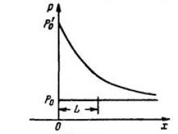
Fig.3.14. The distribution curve of the concentration of non-equilibrium minor
carriers (holes) in the electronic region of the pn junction
If the non-equilibrium concentration is small compared to the concentration of equilibrium main carriers (low level of injection), then the decrease in the concentration of non-equilibrium carriers in the direction from the transition deep into the semiconductor will occur according to an exponential law (Fig. 3.14):
![]() (3.23)
(3.23)
L characterizes the average distance over which the carriers have time to diffuse during their lifetime.
At a point far enough away from the transition (x →¥ ) the equilibrium concentration of charge carriers will be maintained.
At a low level of injection, the concentration of nonequilibrium carriers in n- the region near the interface will depend exponentially on the magnitude of the voltage applied to the junction:
![]() (3.24)
(3.24)
(at U= 0; increases rapidly with increasing positive values U).
Note that the change in voltage at the junction by Δ u will lead to an increase in the concentration of nonequilibrium holes in n- areas, i.e. to a change in charge. The change in charge caused by a change in voltage can be thought of as the action of some capacitance. This container is called diffusion , since it appears due to a change in the diffusion component of the current through the junction.
It can be concluded that diffusion capacitance will manifest itself at direct currents through the junction or at low reverse voltages, when the diffusion current cannot be neglected in comparison with the conduction current.
We represent the diffusion capacity as a change in charge Δ Q, related to the voltage change Δ that caused it u:
and estimate the effect of the current through the junction on the diffusion capacitance.
The total charge of minority nonequilibrium carriers in n-domain can be obtained by integrating the expression (3.23).
A semiconductor diode is an electrically converting semiconductor device with one rectifying electrical junction, having 2 outputs.
The structure of a semiconductor diode with an electron-hole junction and its conventional graphic designation are shown in fig. 1.2, a, b.
The letters p and n denote layers with p-type and n-type conductivities, respectively.
Usually, the concentrations of the majority charge carriers (holes in the p layer and electrons in the n layer) differ greatly. A semiconductor layer with a higher concentration is called an emitter, and a layer with a lower concentration is called a base.

Next, we will look at the main elements of a diode (p-n junction and non-rectifying metal-semiconductor contact), the physical phenomena underlying the operation of the diode, as well as important concepts used to describe the diode.
A deep understanding of physical phenomena and possession of these concepts is necessary not only in order to correctly select specific types of diodes and determine the operating modes of the corresponding circuits, performing traditional calculations using one method or another.
In connection with the rapid introduction of modern circuit simulation systems into engineering practice, these phenomena and concepts have to be constantly kept in mind when performing mathematical modeling.
Simulation systems are rapidly improving, and mathematical models of electronic circuit elements more and more quickly take into account the most "subtle" physical phenomena. This makes it highly desirable to constantly deepen knowledge in the described area and make it necessary to understand the basic physical phenomena, as well as the use of the corresponding basic concepts.
The following description of the main phenomena and concepts, among other things, should prepare the reader for a systematic study of the issues of mathematical modeling of electronic circuits.
The phenomena and concepts considered below must be known when studying not only a diode, but also other devices.
The structure of the p-n-junction.
First, consider the semiconductor layers isolated from each other (Fig. 1.3). 
Let's depict the corresponding zone diagrams (Fig. 1.4). 
In the domestic literature on electronics, the levels of band diagrams and the differences of these levels are often characterized by potentials and potential differences, measuring them in volts, for example, they indicate that the band gap f 5 for silicon is 1.11 V.
At the same time, foreign circuit simulation systems implement the approach that the indicated levels and level differences are characterized by one or another energy and are measured in electron volts (eV), for example, in response to a request from such a system about the band gap in the case of a silicon diode, value 1.11 eV.
In this paper, we use the approach adopted in the domestic literature.
Now consider the contacting layers of the semiconductor (Fig. 1.5). 
In the contacting layers of the semiconductor, there is diffusion of holes from layer p to layer n, the reason for which is that their concentration in layer p is much higher than their concentration in layer n (there is a hole concentration gradient). A similar reason ensures the diffusion of electrons from layer n to layer p.
Diffusion of holes from layer p to layer n, firstly, reduces their concentration in the near-boundary region of layer p and, secondly, reduces the concentration of free electrons in the near-boundary region of layer n due to recombination. The diffusion of electrons from layer n to layer p has similar results. As a result, the so-called depleted layer arises in the near-boundary regions of the p layer and the n layer, in which the concentration of mobile charge carriers (electrons and holes) is low. The depleted layer has a high resistivity.
The impurity ions of the depleted layer are not compensated by holes or electrons. Together, the ions form uncompensated space charges, which create an electric field with a strength E indicated in Fig. 1.5. This field prevents the transition of holes from layer p to layer n and the transition of electrons from layer n to layer p. It creates the so-called drift flow of mobile charge carriers, which moves holes from layer n to layer p and electrons from layer p to layer n.
In steady state, the drift flow is equal to the diffusion flow due to the concentration gradient. In an asymmetric p-n junction, the charge in the layer with a lower impurity concentration, i.e., in the base, is more extended.
Let us depict the band diagram for the contacting layers (Fig. 1.6), taking into account that the Fermi level for them is the same. 
Consideration of the structure of the p-n-junction and the study of the band diagram (Fig. 1.6) show that a potential barrier arises in the region of the transition. For silicon, the height Af of the potential barrier is approximately 0.75 V.
We accept the condition that the potential of some point remote from the transition in the layer p is equal to zero. Let's plot the dependence of the potential Ф on the x-coordinate of the corresponding point (Fig. 1.7). As can be seen from the figure, the value of the coordinate x = 0 corresponds to the boundary of the semiconductor layers. 
It is important to note that the band diagrams presented above and the graph for the potential Ф (Fig. 1.7) strictly correspond to the approach used in the literature on semiconductor physics, according to which the potential is determined for an electron that has a negative charge.
In electrical engineering and electronics, it is defined as the work done by the field forces to transfer a single positive charge.
Let's plot the dependence of the potential Fe, determined on the basis of the electrical approach, on the x coordinate (Fig. 1.8). 
Below, the index "e" in the designation of the potential will be omitted and only the electrotechnical approach will be used (with the exception of zone diagrams).
Direct and reverse inclusion of a p-n-junction. An idealized mathematical description of the transition characteristic.
Connect an external source to the p-n junction as shown in Fig. 1.9. This is the so-called direct inclusion of the p-n-junction. As a result, the potential barrier will decrease by the value u (Fig. 1.10), the drift flux will decrease, the p-n junction will go into a non-equilibrium state, and the so-called forward current will flow through it. 
Connect a source to the p-n junction as shown in Fig. 1.11. This is the so-called reverse inclusion of the p-n junction. Now the potential barrier will increase by u (Fig. 1.12). In the case under consideration, the p-n junction will be very small. This is the so-called reverse, which is provided by the thermal generation of electrons and holes in the regions adjacent to the region of the p-n junction. 
However, space charges create an electric field, which in turn most significantly affects the movement of free electricity carriers, i.e., the process of current flow.
As the inverse increases, the area of space charges (mainly due to the base) and the magnitude of the charge in each layer (p and n) of the semiconductor increase. This increase occurs disproportionately: with a large reverse voltage, the charge increases with an increase in the module more slowly than with a small reverse voltage.
Let's give an explanatory illustration (Fig. 1.19), where we use the notation:
Q is the space charge in the layer n of the semiconductor;
u is the external voltage applied to the p-n junction. 
Denote by f the function describing the dependence of Q on u. In accordance with the above
In the practice of mathematical modeling (and in manual calculations), it is convenient and therefore customary to use not this expression, but another, obtained from this as a result of differentiation. In practice, the so-called barrier capacitance C 6ar p-n junction is widely used, and by definition C 6ar = | dQ / du | Let's draw graphs for Q (Fig. 1.20) and C bar (Fig. 1.21). 
The phenomenon of the emergence and change of the volume charge of non-equilibrium carriers of electricity. diffusion capacity.
If an external source shifts the p-n junction in the forward direction (u> 0), then injection (emission) begins - the entry of minority carriers of electricity into the semiconductor layer under consideration. In the case of an asymmetric p-n junction (which usually happens in practice), the main role is played by injection from the emitter into the base.
Further, we assume that the junction is not symmetrical and that layer p is the emitter and layer n is the base. Then injection is the entry of holes into layer n. The consequence of injection is the appearance of holes in the space charge base.
It is known that in semiconductors the phenomenon of dielectric relaxation (Maxwell relaxation) takes place, which consists in the fact that the space charge that has arisen is almost instantly compensated by the charge of the approaching free carriers of a different sign. This happens in the order of 10 -12 s or 10 -11 s.
In accordance with this, the charge of holes entering the base will be almost instantly neutralized by the electron charge of the same modulus.
We use the notation:
Q is the space charge of nonequilibrium carriers in the base;
u is the external voltage applied to the p-n junction;
f is a function describing the dependence of Q on u.
Let's give an explanatory illustration (Fig. 1.22). 
In accordance with the above, Q = f(u) In practice, it is convenient and customary to use not this expression, but another, obtained from this as a result of differentiation. In this case, the concept of diffusion capacitance C diff p-n junction is used, and by definition C diff \u003d dQ / du The capacitance is called diffusion, since the considered charge Q underlies the diffusion of carriers in the base.
C diff is convenient and customary to describe not as a function of u, but as a function of the current i of the p-n junction.
The charge Q itself is directly proportional to the current i (Fig. 1.23, a). In turn, i exponentially depends on u (the corresponding expression is given above), so the derivative di / du is also directly proportional to the current (for an exponential function, its derivative is greater, the greater the value of the function). It follows that the capacitance C diff is directly proportional to the current i (Fig. 1.23.6):
Cdif=i τ/φt where φt is the temperature potential (defined above);
τ is the mean time of flight (for a thin base), or lifetime (for a thick base).
The mean time of flight is the time during which the injected electricity carriers pass through the base, and the lifetime is the time from the injection of the electricity carrier into the base to recombination.
The total capacitance of the p-n junction.
This capacitance C lane is equal to the sum of the considered capacities, i.e. C lane \u003d C bar + C diff.
When the transition is reverse-biased (u< 0) диффузионная емкость практически равна нулю и поэтому учитывают барьерную емкость. При прямом смещении обычно С бар < С диф.
Non-rectifying metal-semiconductor contact.
To connect external leads in diodes, so-called non-rectifying (ohmic) metal-semiconductor contacts are used. These are such contacts, the resistance of which practically does not depend on either the polarity or the magnitude of the external voltage.
Obtaining non-rectifying contacts is no less important task than obtaining p-n junctions. For silicon devices, aluminum is often used as the contact metal. The properties of a metal-semiconductor contact are determined by the difference between the electron work functions. The work function of an electron from a solid body is the increment in energy that an electron at the Fermi level must receive in order to exit this body.
Let us denote the work function for a metal as A m, and for a semiconductor - as A p. Dividing the work function by the electron charge q, we obtain the corresponding potentials:
φ m =A m /q,φ n =A n /q
Let us introduce into consideration the so-called contact potential difference φ mn:φ mn=φ m -φ n
For definiteness, let us turn to the n-type metal-semiconductor contact. To obtain a non-rectifying contact, the condition φ mn< 0. Изобразим соответствующие зонные диаграммы для неконтактирующих металла и полупроводника (рис. 1.24). 
As follows from the diagram, the energy levels in a semiconductor corresponding to the conduction band are less filled than in a metal. Therefore, after the connection of the metal and the semiconductor, part of the electrons will pass from the metal to the semiconductor. This will lead to an increase in the electron density in the n-type semiconductor.
Thus, the conductivity of the semiconductor in the contact region will be increased and the layer depleted of free carriers will be absent. This phenomenon is the reason that the contact will be non-rectifying. To obtain a non-rectifying p-type metal-semiconductor contact, it is necessary to fulfill the condition φmp> 0
When an alternating voltage is applied to the p-n-junction, capacitive properties appear.
The formation of a p-n junction is associated with the appearance of a space charge created by immobile ions of donor and acceptor atoms. An external voltage applied to the p-n junction changes the value of the space charge in the junction. Consequently, the p-n junction behaves like a kind of flat capacitor, the plates of which are the n- and p-type regions outside the junction, and the space charge region, depleted in charge carriers and having high resistance, is the insulator.
Such a capacitance p-n-junction is called barrier. The barrier capacitance C B can be calculated by the formula
S - p-n-junction area; 0 - relative () and absolute ( 0) permittivity; - p-n junction width.
A feature of the barrier capacitance is its dependence on the external applied voltage. Taking into account (2.2), the barrier capacitance for a sharp transition is calculated by the formula:
 ,
,
where the sign “+” corresponds to the reverse, and “-“ to the forward voltage at the junction.
rice. 2.6 Barrier capacitance versus reverse voltage 
Depending on the junction area, dopant concentration, and reverse voltage, the barrier capacitance can take values from units to hundreds of picofarads. Barrier capacitance appears at reverse voltage; at direct voltage, it is shunted by a small resistance r pn.
In addition to the barrier capacitance, the p-n junction has the so-called diffusion capacitance. Diffusion capacity is associated with the processes of accumulation and resorption of a non-equilibrium charge in the base and characterizes the inertia of the movement of non-equilibrium charges in the base region.
Diffusion capacity can be calculated as follows:
 ,
,
where t n is the lifetime of electrons in the base.
The value of diffusion capacitance is proportional to the current through the p-n junction. With a forward voltage, the value of the diffusion capacitance can reach tens of thousands of picofarads. The total capacitance of the p-n junction is determined by the sum of the barrier and diffusion capacitances. With reverse voltage C B > C DIF; at forward voltage, the diffusion capacitance C DIF >> C B prevails.

Rice. 2.7 Equivalent circuit p-n-junction on alternating current
In the equivalent circuit, two capacitances C B and C DIF are connected in parallel to the differential resistance of the p-n junction r pn; in series with r pn, the volume resistance of the base r B is included.
With an increase in the frequency of the alternating voltage applied to the p-n junction, the capacitive properties become more and more pronounced, r pn is shunted by the capacitance and the total resistance of the p-n junction is determined by the volume resistance of the base. Thus, at high frequencies, the p-n junction loses its non-linear properties.
Methods for obtaining p - n-Transition
Alloy junctions are obtained by depositing on a semiconductor crystalline substrate a "hatch" of a low-melting metal alloy, which includes the necessary alloying substance. When heated, a region of liquid melt is formed, the composition of which is determined by the joint melting of the sample and the substrate. Upon cooling, recrystallization is formed. A region of a semiconductor enriched in dopant atoms. If the type of doping of this region is different from the type of doping of the substrate, then a sharp p - n-transition, and its metallurgical boundary X 0 coincides with the recrystallization boundary of the region. In alloy transitions on this surface, the difference changes abruptly (sharp p - n-transition). When drawn from the melt, the formation of the transition occurs during the growth of a semiconductor ingot by a dosed change in the composition of dopants in the melt. Diffusion transitions are obtained by diffusion of dopants from sources in the gaseous, liquid and solid phases. Implanted junctions are formed during ionic dopant implantation. Epitaxial transitions are obtained by the method of epitaxial growth or growth, including the method of molecular beam epitaxy, which makes it possible to control the law of change in the most subtle way (with a resolution of up to 1 nm). N D ( x)-N a ( x). Combined methods are often used: after fusion, implantation, or epitaxial growth, diffusion finishing of the structure is performed. Upon receipt p - n-P. not only alloying is regulated R- and n-areas, but also the structure of the entire transition layer; in particular, the required gradient is obtained a = d(N D - N a) /dx at the point of metallurgical transition X = X 0 . In most cases, asymmetric R + - P- or P + - r -P., in which the doping of one of the regions (+) is much stronger than the other.
Applications p - n-P. has a non-linear CVC with a large rectification coefficient, on which the action of rectifier (semiconductor) diodes is based. By changing the thickness of the depleted layer with a change in voltage U it has a controlled non-linear capacitance.
Turned on in the forward direction, it injects carriers from one of its regions to another. Injected carriers can control current etc. p - n-transition, recombine with light emission, turning p - n-Transition. into an electroluminescent radiation source, inertially linger in the injection area during fast voltage switching to R - n-P. Current p - n-P. controlled by light or other ionizing radiation. Properties p - n-P. determine their use in decomp. devices: rectifier, detector, mixing diodes, bipolar and unipolar transistors; tunnel diodes; avalanche-span diodes (microwave generators); photodiodes, avalanche photodiodes, phototransistors ; thyristors, photothyristors; photocells, solar batteries; LEDs, injection lasers; particle detectors, etc. R - n-junction are displaced by Schottky barriers, isotype heterojunctions, and planar-doped barriers.
When an alternating voltage is applied to the p-n-junction, capacitive properties appear.
The formation of a p-n junction is associated with the appearance of a space charge created by immobile ions of donor and acceptor atoms. An external voltage applied to the p-n junction changes the value of the space charge in the junction. Consequently, the p-n junction behaves like a kind of flat capacitor, the plates of which are the n- and p-type regions outside the junction, and the space charge region, depleted in charge carriers and having high resistance, is the insulator.
Such a capacitance p-n-junction is called barrier . The barrier capacitance C B can be calculated by the formula
S - p-n-junction area; e e 0 - relative (e) and absolute (e 0) permittivity; D is the width of the p-n junction.
A feature of the barrier capacitance is its dependence on the external applied voltage. Taking into account (2.2), the barrier capacitance for a sharp transition is calculated by the formula:
 ,
,
where the sign “+” corresponds to the reverse, and “-“ to the forward voltage at the junction.

The dependence of the barrier capacitance on the reverse voltage is called the capacitance-voltage characteristic (see Fig. 2.6). Depending on the junction area, dopant concentration, and reverse voltage, the barrier capacitance can take values from units to hundreds of picofarads. Barrier capacitance appears at reverse voltage; at direct voltage, it is shunted by a small resistance r pn.
In addition to the barrier capacitance, the p-n junction has the so-called diffusion capacitance. Diffusion capacity is associated with the processes of accumulation and resorption of a non-equilibrium charge in the base and characterizes the inertia of the movement of non-equilibrium charges in the base region.
Diffusion capacity can be calculated as follows:
 ,
,
where t n is the lifetime of electrons in the base.
The value of diffusion capacitance is proportional to the current through the p-n junction. With a forward voltage, the value of the diffusion capacitance can reach tens of thousands of picofarads. The total capacitance of the p-n junction is determined by the sum of the barrier and diffusion capacitances. With reverse voltage C B > C DIF; at forward voltage, the diffusion capacitance C DIF >> C B prevails.

The equivalent circuit of the p-n-junction on alternating current is shown in fig. 2.7. In the equivalent circuit, two capacitances C B and C DIF are connected in parallel to the differential resistance of the p-n junction r pn; the volume resistance of the base r¢ B is connected in series with r pn. With an increase in the frequency of the alternating voltage applied to the p-n junction, the capacitive properties become more and more pronounced, r pn is shunted by the capacitance and the total resistance of the p-n junction is determined by the volume resistance of the base. Thus, at high frequencies, the p-n junction loses its non-linear properties.
Diode types
Diodes are classified:
1. By frequency:
2. low-frequency;
3. midrange;
4. high-frequency;
5. Microwave - diodes.
6. By manufacturing technology:
7. point;
8. floatable;
9. diffusion.
10. By functional purpose:
11. rectifier;
12. universal;
13. LEDs;
14. tunnel diodes.
The main characteristics of a rectifier diode are the following parameters: I pr, U pr, I pr max, U pr max, I arr, U arr max, r dif, where r diff– differential resistance of the diode: .
For a zener diode, the main parameters are I with min , I with max , U with min , U with max, besides the zener diode (determined at the operating point), ratings and breakdown voltage U arr max. TKN (Temperature Coefficient of Stress) is also given:  or in %
on the °C:
or in %
on the °C:  .
.
Pulse diodes are characterized by an operating frequency f and impulse response: t east(the time during which the diode restores its properties), the capacitance of the p-n junction Cpn and the same characteristics as rectifier diodes: I pr, I arr etc.
Power supply system. Classification and characteristics of rectifiers. Single and full wave rectifier with R load.
Power supplies make up the bulk of an electronic device. About 50% from the weight of the equipment is the power supply due to the fact that it usually includes a transformer, which has large dimensions and weight.
The power supply consists of: transformer, diode circuit, smoothing filter and stabilizer .
Power supply system - a set of primary and secondary power sources.
Primary Power Sources - devices that convert non-electric energy into electrical energy (generators, etc.)
Secondary power supplies - devices that convert one type of electrical energy into another (for example, alternating current to direct current ( rectifiers ), DC to AC ( inverters )).
Transformer designed to match the diode circuit with the supply network. The ratio of the number of turns of the secondary and primary windings is called transformation ratio. The second purpose of the transformer is to isolate the diode circuit from the network if the load is grounded.
diode circuit designed to rectify the voltage at the input and obtain a certain constant component at the output.
U d is the constant component of the voltage;
I d is the constant component of the current.
Depending on the type of diode circuit, the quality of the voltage at the output of the diode circuit is different. This quality evaluates the ripple factor:
 .
.
The ripple factor can be either greater than 1 (for full-wave rectifiers) or less than 1 (for half-wave rectifiers).
Passive RC and LC filters are used as smoothing filters (LC filters are more often used). One LC filter element reduces the ripple factor by no more than 25 times. For a stronger reduction K p apply 2 or 3-link filters. (if the number of links is more than 3, self-excitation is possible).
Stabilizer designed to further reduce ripple (reduces K p 1000 times or more). As a rule, its basis is integrated circuits (op-amps or special circuits).
The combination of a transformer, a diode circuit, and a smoothing filter is called rectifier . The main characteristics of the rectifier are:
1) medium rectified current at the load I 0;
2) medium rectified voltage at the load U 0;
3) ripple factor at the load K n0;
4) external characteristic of the rectifier U 0 \u003d U 0 (I 0).
Half-wave rectifier circuit.
 |
 |
We will show the processes occurring in the circuit on oscillograms:
In the positive half cycle voltage U 2 diode VD opens and current flows through the load i 2 equal i d. At the same time, the voltage on the load has a sinusoidal character with an amplitude U 2 m(we neglect the voltage drop across the diode).
In the negative half cycle voltage U 2 diode VD is closed and a reverse voltage is applied to it U arr max \u003d U 2 m. Thus, the voltage and current on the load are pulsed (from 0 to p– sinusoidal character and from p before 2p voltage and current are zero).
Let's define the characteristics of the rectifier:
1. Operating voltage of the secondary winding of the transformer:
denote wt=u, then  or
or ![]() .
.
From here, the disadvantage of a half-wave rectification circuit is immediately visible: the average rectified voltage of the winding is more than 2 times less U 2.
, where I 2m- the amplitude of the current of the secondary winding of the transformer.
Knowing the relationship between U d and U 2 you can write the following expression:
I 2 \u003d 1.57I d,where I d- average rectified current.
These expressions allow you to determine the power of the secondary winding of the transformer, as well as obtain the requirements for the winding wire of the secondary winding ( P 2 \u003d U 2 I 2).
3. The effective value of the current of the primary winding of the transformer:
between the current of the primary and secondary windings, the relationship is linear, where n- transformation coefficient. In its turn i 2 \u003d I 2 -I d, then ![]() . Let's determine the effective value of the current i 1 (I 1):
. Let's determine the effective value of the current i 1 (I 1):
.
Next, you can determine the power P1 transformer primary winding ( P 1 \u003d U 1 I 1). Knowing the power of the primary and secondary windings, you can calculate the typical power of the transformer ( S): ![]()
4. Reverse voltage across the diode ![]()
5. The frequency of the first harmonic of the voltage at the load ( f n1): f n1 \u003d f networks \u003d 50 Hz.
This implies the second drawback of the half-wave rectification circuit. It consists in the fact that at a frequency 50Hz when constructing an anti-aliasing filter, more cumbersome L and C are needed.
6. Pulsation coefficient , where U 1 m is determined by expanding the load voltage curve into a Fourier series (for a half-wave rectification circuit U 1 m > U d, which is also its disadvantage).
Because in the current of the secondary winding there is a constant component equal to I d, then the transformer experiences a forced bias, therefore, the signal at the output of the transformer may be distorted due to its saturation. To avoid this, increase the size of the transformer.
In connection with the listed shortcomings, this scheme is used if high quality of the output signal is not required.
Full-wave circuit with a midpoint.
It contains a medium-terminal transformer and two diodes. Consists of two half-wave rectifiers.

W ’ 2 \u003d W ’’ 2; 
Its disadvantage is immediately visible from the circuit: the need to output the midpoint of the transformer and the same number of turns of the secondary winding.
 |
Let's draw the timing diagrams:
Let's consider the operation of this scheme.
In the positive half-cycle, the VD1 diode is open and the diode current flows through the load i d1. Load voltage amplitude U n max \u003d U 2 m. In the negative half-cycle, the VD1 diode closes and the VD2 diode opens, since the half-windings are identical, the voltage amplitude at the load will also be equal to U 2 m. The voltage at the load has a pulsed character, and the frequency of the fundamental harmonic is 2 times higher than the mains frequency ( f n1 \u003d 2f network). The current flowing in each of the half-windings is different from zero during one half-cycle. With respect to the core of the transformer, the magnetic fluxes created by the currents of the half-windings are sinusoidal. Therefore, we can assume that the current of the secondary winding of the transformer (relative to the core) has a sinusoidal character.
The main characteristics of the rectifier.
1. Medium rectified voltage at the load U d:
because this rectifier is a combination of two half-wave rectifiers, then: .
2. The effective value of the current of the secondary winding of the transformer:
because the nature of the current flowing through the half-winding of the transformer (in comparison with a half-wave rectifier) has not changed, then the ratio will be the same: .
Further, having made similar conclusions as for a half-wave rectifier, we obtain:
The disadvantages of the circuit include the complexity of the circuit and the design of the transformer.
A semiconductor diode is inert with respect to sufficiently rapid changes in current or voltage, since a new carrier distribution is not immediately established. As is known, an external voltage changes the width of the junction, and hence the magnitude of the space charges in the junction. In addition, during injection or extraction, the charges in the base region change (the role of charges in the emitter is insignificant). Therefore, the diode has a capacitance that can be considered connected in parallel with the p-n junction. This capacity can be divided into two components: barrier capacity, reflecting the redistribution of charges in the transition, and diffusion capacity, reflecting the redistribution of charges in the base. Such a division is generally conditional, but it is convenient in practice, since the ratio of both capacitances is different for different polarities of the applied voltage. With a forward voltage, the main role is played by excess charges in the base and, accordingly, by the diffusion capacitance. When the voltage is reversed, the excess charges in the base are small and the barrier capacitance plays the main role. We note in advance that both capacitances are not linear: the diffusion capacitance depends on the forward current, and the barrier capacitance depends on the reverse voltage.
Let us determine the value of the barrier capacitance, considering the transition as asymmetric type n + -p. Then the extent of the negative charge in the p-type base can be considered equal to the entire width of the transition: . Let's write the module of this charge:
where N is the impurity concentration in the base; S - transition area. The same (but positive) charge will be in the emitter layer.
Imagine that these charges are located on the plates of an imaginary capacitor, the capacitance of which can be defined as
Taking into account the expression for the width of the transition during reverse switching, and differentiating the charge Q with respect to voltage, we finally obtain:
 (7.10)
where and are, respectively, the width and height of the potential barrier in the equilibrium state.
Keeping in mind that the diode has a capacitance, you can draw up its complete equivalent circuit for alternating current (Fig. 3.10a).

The resistance R 0 in this circuit represents the total relatively small resistance of the n- and p- regions and the contacts of these regions with the leads. The non-linear resistance R nl with direct connection is equal to R pr, i.e. is small, and at reverse voltage R nl = R arr, i.e. it is very big. The given equivalent circuit in various frequency cases can be simplified. At low frequencies, the capacitance is very large and the capacitance can be ignored. Then, with a forward bias, only the resistances R 0 and R pr remain in the equivalent circuit (Fig. 7.5b),

Fig.7.5b. Fig. 7.5c.
and with a reverse voltage - only the resistance R arr, since R 0<< R обр (рис.7.5в).
At high frequencies, capacitances have relatively little resistance. Therefore, with a forward voltage, a circuit is obtained according to Fig. 7.5d, (if the frequency is not very high, then C diff has practically no effect),

Fig.7.5d. Fig. 7.5e.
and in the opposite case, R arr and C b remain (Fig. 7.5e).
It should be borne in mind that there is still capacitance C in between the terminals of the diode, which can significantly shunt the diode at very high frequencies. The inductance of the leads can also appear on the microwave.
Classification of diodes.
The classification of diodes is carried out mainly:
1) on technological methods for creating electrical junctions and diode structures
2) according to the function of the diodes.
According to the manufacturing technology, diodes can be point and planar. The main characteristics of point diodes: the p-n-junction area is small, they have a small capacitance (less than 1pF), low currents (no more than 1 or tens of mA). Used at high frequencies up to microwave. Technology: a tungsten filament coated with an acceptor impurity (for germanium - indium, for silicon - aluminum) is welded to a plate of n-type germanium or n-type silicon using a large current pulse.
Planar diodes: manufacturing technology can be either fusing or diffusion. When fusing, a tablet of metal acceptor material, such as aluminum, is placed on the cleaned surface of a semiconductor wafer, usually n-type, if the semiconductor is silicon. When heated to 600 ... 700 0 C, it melts and dissolves the adjacent layer of silicon, the melting point of which is much higher. After cooling near the surface of the plate, a p + -type silicon layer saturated with aluminum (p-type emitter, n-type base). Diffusion: impurity atoms usually come from a gaseous medium into a semiconductor plate through its surface at a high temperature (about 1000 0) and propagate in depth due to diffusion, i.e. thermal movement. The process is carried out in special diffusion furnaces, where the temperature and time of the process are maintained with high accuracy. The longer the time and temperature, the further the impurities penetrate into the depth of the plate. The diffusion pn junction turns out to be flat, and its area is large and equal to the area of the original plate, the operating currents reach tens of amperes.
According to the function performed, rectifier, pulse, converter, switching, detector diodes, zener diodes, varicaps, etc. are distinguished. Separate classes of diodes can be subdivided into subclasses depending on the operating frequency range (low-frequency, high-frequency, microwave diodes, diodes of the optical range). Diodes are also distinguished by semiconductor material: silicon is most widely used, replacing the previously common germanium. Silicon diodes have a higher maximum operating temperature (Si - 125 ... 150 0 C, Ge - 70 ... 80 0 C) and several orders of magnitude lower reverse current. The number of gallium arsenide diodes (in particular, metal-semiconductor ones), which are superior in parameters to silicon diodes, is constantly increasing.
Consider some types of diodes and their main parameters.
1.Rectifier low frequency diodes. They are used in AC power supplies.
The main electrical parameters of the diode are the values of U ex.avg at a given I ex.avg, as well as I arr.avg at a given amplitude (maximum) value of the reverse voltage (U arr.max) values of forward voltage and reverse current for the period). For silicon diodes with a p-n junction, which are most common, U ave.av does not exceed 1..1.5V at T \u003d 20 0 C. With increasing temperature, this value decreases, and TKN depends on the value of the forward current; decreases with increasing current, and at high current it can even become positive. The reverse current of silicon diodes at T = 20 0 C, as a rule, does not exceed tenths of μA, and increases with increasing temperature (the doubling temperature is about 10 0 C). At T=20 0 C, the reverse current can be neglected. The breakdown voltage of silicon diodes is hundreds of volts and increases with increasing temperature.
The forward voltage of silicon diodes with a metal-semiconductor junction is approximately two times less than in diodes with a p-n junction. And the reverse current is somewhat larger and more strongly dependent on temperature, doubling for every 6..8 0 С.
When choosing the type of diode, the maximum allowable rectified current, reverse voltage and temperature are taken into account. Depending on the allowable current, diodes of small (<300мА), средней (<1А) и большой (>10A) power. The limiting reverse voltage is limited by the breakdown of the transition and lies in the range from 50 to 1500V. To increase the allowable reverse voltage, the diodes are connected in series. Several diodes connected in series, manufactured in a single technological cycle and enclosed in a common housing, are called a rectifier pole. The maximum operating temperature of silicon diodes reaches 125..50 0 C and is limited by the growth of the reverse current.
Low-power diodes with a small p-n junction area (less than 1 mm 2) are created by fusing, high-power ones with a large area - by diffusion. Power diodes with a p-n junction can operate up to frequencies usually not more than 1 kHz, and diodes with a metal-semiconductor junction - up to frequencies of hundreds of kHz.
Germanium diodes have a forward voltage approximately 1.5..2 times less than silicon diodes (usually no more than 0.5 V) due to the smaller band gap. It is mainly determined by the voltage drop across the base resistance, in this case, TC U pr >0. The reverse current at T=20 0 C is 2..3 orders of magnitude greater than in silicon diodes, and depends more strongly on temperature. Doubling for every 8 0 C, in connection with this, the maximum operating temperature is much lower (70 ... 80 0 C).
The thermal breakdown mechanism leads to the fact that germanium diodes fail even with short-term impulse overloads. This is a significant disadvantage. The breakdown voltage decreases with increasing temperature.
Due to the small junction area, the maximum allowable direct currents of high-frequency diodes are small (usually less than 100mA), breakdown voltages, as a rule, do not exceed 100V.
3. pulse diodes. Designed for operation in pulsed mode, i.e. in devices for the formation and conversion of pulse signals, key and digital circuits.
The most important parameter of pulsed diodes is the recovery time of the reverse resistance. It characterizes the transitional process of switching the diode from a state with a given forward current I CR to a state with a given reverse voltage U arr. Figure 7.6 shows the timing diagrams of voltage and current through the diode.

The recovery time t is counted from the moment t 1 of the voltage change on the diode from direct to reverse until the moment t 2 when the reverse voltage reaches a value of 0.1 ave. moment t 1), as well as the process of recharging the barrier capacitance. In switching diodes, the recovery time should be as short as possible; it is necessary to reduce the lifetime of minority carriers in the base, for which silicon diodes with a p-n junction are doped with gold. But for silicon diodes, it is not possible to obtain a recovery time of the order of less than 1 ns. In gallium arsenide, the lifetime is much shorter than in silicon, and in diodes with a p-n junction, it is possible to obtain t res of the order of 0.1 ns. The reduction in barrier capacitance is achieved by reducing the transition area. The shortest recovery time (t re<0.1нс) имеют диоды с переходом металл-полупроводник, в которых отсутствует накопление неосновных носителей при протекании прямого тока. В них время восстановления порядка C б r б определяется процессом перезаряда барьерной емкости перехода через сопротивление базы.
For all pulse diodes, the capacitance is specified at a certain reverse voltage and frequency of the AC signal used in the measurement. The minimum capacitance values are 0.1…1 pF.
The specific parameters of pulsed diodes include the maximum pulse reverse current I rev.i.max and the maximum impulse resistance r pr.i.max, equal to the ratio of the maximum forward voltage in the process of its establishment to the forward current. It is desirable to have the values of these quantities as small as possible.
For pulsed diodes, static parameters are also important, which determine the steady-state values of current and voltage in the circuits. These include forward voltage at a given forward current and reverse current at a given reverse voltage.
4. Zener diodes. A zener diode is a semiconductor diode designed to stabilize voltages in circuits. Zener diodes are used in power supplies, limiters, level clamps, voltage references and other devices. The principle of operation of zener diodes is based on the use of avalanche or tunnel breakdown in the p-n junction. Figure 7.7 shows a typical volt-ampere characteristic of a zener diode with reverse voltage.

In the breakdown section - the working section of the CVC, the voltage depends very weakly on the current. The minimum value of the operating current I st.min corresponds to the beginning of the "vertical" section of the I–V characteristic, where a small differential resistance r diff =ΔU/ΔI is achieved. The maximum current I st.max is determined by the allowable power dissipation. The main parameter is the stabilization voltage U st, which is practically equal to the breakdown voltage, is set at a certain value of the current I st in the working area.
 The zener diode switching circuit is shown in Fig. 7.8.
Here R ogr is a limiting resistor; R n - load resistor, the voltage at which U n \u003d U st. The current flowing through the limiting resistor is I \u003d (E-U st) / R ogr, and the current through the zener diode I st \u003d I-I n, where I n \u003d U st / R n, which corresponds to the operating point c in Fig. 3.11. If the power supply voltage deviates by an amount from the nominal value, the current through the zener diode changes by Δ I st = ΔE) / R limit at r diff<<(R огр ││ R н) и рабочая точка перемещается в пределах участка C ’ C”; напряжение на нагрузке изменяется на очень малую величину
 (7.11)
If the load current changes and therefore, the load on the value of Δ I n, then the current through the zener diode and Δ U \u003d - r diff ΔI n will change in approximately the same way. The “-” sign means that as the load current increases, the zener diode current decreases. To obtain good stabilization, the differential resistance should be as low as possible.
The breakdown voltage of the p-n junction decreases with an increase in the concentration of base impurities. For devices of various types, U st can be from 3 to 200V.
The effect of temperature is estimated by the temperature coefficient of the stabilization voltage of the TKN, which characterizes the change in voltage U st with a change in temperature by one degree, i.e.
 (7.12)
Voltage temperature coefficient can be from 10 -5 to 10 -3 K -1 . The value of U article and the sign of TKN depend on the resistivity of the main semiconductor. Zener diodes for voltages up to 7V are made of silicon with low resistivity, i.e. with a high concentration of impurities. In these zener diodes, the p-n junction has a small thickness, a field with a high intensity acts in it, and the breakdown occurs mainly due to the tunnel effect. In this case, the TKN turns out to be negative. If silicon with a lower concentration of impurities is used, then the p-n junction will be thicker. Its breakdown occurs at higher voltages and is an avalanche. Such zener diodes are characterized by a positive TKN.
The temperature coefficient of stabilization of high-voltage zener diodes can be reduced by 1 ... 2 orders of magnitude, using thermal stabilization. To do this, the back-connected p-n junction of the zener diode is connected in series with one or two p-n junctions connected in the forward direction. It is known that the forward voltage at the p-n junction decreases with increasing temperature, which compensates for the increase in breakdown voltage. Such thermally compensated zener diodes are called precision. They are used as reference voltage sources.
Most often, the zener diode operates in such a mode when the source voltage is unstable, and the load resistance R n is constant. To establish and maintain the correct stabilization mode in this case, the resistance R limit must have a certain value. Usually R ogr is calculated for the midpoint with the characteristics of the zener diode. If the voltage E changes from E min to E max, then R limit can be found using the following formula
 (7.13)
where E cf \u003d 0.5 (E min + E max) - the average voltage of the source;
I cf \u003d 0.5 (I min + I max) - the average current of the zener diode;
I n \u003d U st / R n - load current.
If the voltage E begins to change in one direction or another, then the current of the zener diode will change, but the voltage on it, and therefore on the load, will be almost constant. Since all changes in the source voltage must be absorbed by the limiting resistor, the largest change in this voltage, equal to E max - E min , must correspond to the largest possible change in current, at which stabilization is still preserved, i.e. I max - I min. It follows that if the value of E changes by ΔE, then stabilization will be carried out only if the condition
The second possible stabilization mode is used when E=const, and R n varies from R n min to R n max . For such a regime, R limit can be determined from the average values of the currents according to the formula
 (7.15)
I n cf \u003d 0.5 (I n min + I n max), and I n min \u003d U st / R n max and I n max \u003d U st / R n min.
To obtain higher stable voltages, a series connection of zener diodes designed for the same currents is used.
5. Varicaps. Diodes are called varicaps, the principle of operation of which is based on the dependence of the barrier capacitance of the p-n junction on the reverse voltage. Thus. Varicaps are capacitors of variable capacity, controlled not mechanically, but electrically, i.e. reverse voltage change. They are used as elements with electrically controlled capacitance in frequency tuning circuits of an oscillatory circuit, frequency division and multiplication, frequency modulation, controlled phase shifters, etc.
The simplest circuit for switching on a varicap to adjust the frequency of the oscillatory circuit is shown in Fig. 7.9.

The control voltage U is applied to the varicap VD through a high-resistance resistor R, which reduces the shunting of the varicap and the oscillatory circuit by the voltage source. To eliminate the direct current through the inductance element, the oscillatory circuit is connected in parallel to the varicap through a high-capacity separating capacitor Cp. By changing the magnitude of the reverse voltage and, consequently, the capacitance of the varicap and the total capacitance of the oscillatory circuit, the resonant frequency of the latter is changed.
The main semiconductor material for the manufacture of the varicap is silicon, gallium arsenide is also used, which provides a lower base resistance.
The electrical parameters of the varicap include capacitance at nominal, maximum and minimum voltages, measured at a given frequency, capacitance overlap coefficient, quality factor, frequency range, temperature coefficients of capacitance and quality factor. In different types of varicaps, the nominal capacitance can range from a few units to several hundred picofarads.