Processor history. The formation of AMD as a global brand in the microprocessor market Make amd processors
Throughout the existence of the company, and this is more than 40 years, the global brandAMDnever managed to become the most popular manufacturer of semiconductor devices and microprocessors.
However, these 40 years have not gone unnoticed by the microprocessor market.
The history of the creation, development and existence of a global brand is interesting not only because it significantly affected semiconductor devices and microprocessors
but also as an example of how you can compete on equal terms with a leading company that surpasses you both technologically and financially.
Indeed, as competitors to the global brandIntel, were much more serious companies thanAMD. But today onlyAMDcan offer a quality product alternativeIntel.

How it all began
It all started with Jerry Sanders, who studied at the University of Illinois as an electronic engineer with a naive dream - to become a movie star in the future.
It was not possible to become a movie star, but his whole life until the beginning of the 21st century was connected with the then non-existent global brandAMD.
After successfully graduating from university in 1958, Jerry got a job at Douglas Aircraft, but a career in engineering was not close to his heart.
Therefore, the very next year, Jerry worked inMotorolanot an engineer, but an employee of the sales and marketing department. VMotorolahe also did not stay long, and in 1961 Sanders was in sales and marketing for Fairchild Semiconductor.
Fairchild Semiconductor is a company that is listed in the stories of many of the founders of today's global brands.
Most likely, due to the fact that Fairchild Semiconductor at that time created transistors that were very successfully sold, it was difficult not to notice the high prospects of this activity.
Having gained invaluable experience in the field of development and sales in 1968, Gordon Moore, Bob Noyce and Andy Grove, who, it is worth noting, worked on the same team as Jerry Sanders, leave the company to found Intel.
Sanders, in turn, as director of sales, leaves the company to head his own commercial semiconductor company.

Apparently, all these people saw a great prospect in the semiconductor industry, to separate from Fairchild Semiconductor and organize their own, now global, brands.
As it turns out later, they did not lose.After all, today we see them as the fiercest competitors forworldindustry leadership.
Jimmy Sanders, May 1, 1969 created a company with 8 like-minded peopleAMD(Advanced Micro Devices), their capital at that time was 100 thousand dollars. Sanders was not a talented engineer, but he assembled an excellent engineering team and relied on his ability to sell.
At first, the company was in the living room of one of the co-founders John Carey, then it moved to a rented two-room apartment.
And by September 1969, the company moved to its first permanent address in the California town of Sunnyvale (Sunnyvale). There, the company's first production at Fab1 began.
At first, the company was unable to develop or produce its own unique products,AMDspecialized in redesigned products from other companies.
Memory registers, chips, and power supplies were purchased from third-party firms, then modified to increase efficiency and superiority over similar products from other manufacturers, and were sold at a relatively low price.
To attract the attention of buyers, AMD conducted tests of its modifications to meet the stringent standards of US Army customers. It was more profitable for consumers to purchase products whose quality level was acceptable for the military, at a cost slightly higher than analogues.
"Military" quality at the expense of the company is the slogan AMD brings to the buyer.
Sanders' technique worked. A year after the start of its activities, the number of employees of the organization exceeded 50 people.
1972 The global brand AMD publicly issues shares, and in early 1973, the first large-scale chip production from scratch was opened in Malaysia.
The company grew rapidly, and after 5 years the staff exceeded 1500. The company had about 200 products, and sales exceeded $ 26 million. At the time, this was AMD's biggest take-off, and it grew, gradually rising to a higher level.
Thanks to Jerry Sanders, in the first 5 years the company stood out for its aggressive nature, the ability to maneuver and use bold and innovative solutions in its activities. Sanders can be said to express his personality at AMD.
Despite the unstable situation on the market and the general fall in prices, there is a steady growth of the company. For each subsequent year, capital growth increased by an average of 60%, and sales volumes approached the $200 million mark.
The capacity of the plant in Penang in Malaysia has grown rapidly, and a new subsidiary in the Philippines has also been opened. In 1974, the global brand AMD released its first Am9102 RAM memory chip.
This yearAMDreleases the first cloneIntel i8080A,morein two yearscross-licensing agreement with Intel. 1979 - companyAMDis listed on the NYSE (New York Stock Exchange), that is, on the list the best companies and launchesown factory in Austin, Texas.
In the 80scompanyAMDhas become a global brand, known throughout the world today as the largest manufacturer of microprocessors.
This was made possible by an extension in 1981cross-licensing agreementsWithIntel, and in 1982 the signing of a new technology exchange agreement.
BecauseIntelno one could imagine an alternative, then, according to the terms of the company's contract, it was necessary to have at least some competition.
Intelthere was nothing left to docreate competition for yourselfamd,leading to fierce competition in the future.Inteldid not take into account thatAMDthere is character and for this the company had to pay in full later.
global brand AMD
![]()
After the signing of the contracts, at the disposalAMDhad access to copying and cloning developmentsIntel.So coming out soon exact copy i286,only with titleAm286.
Differences only in the ability to emulateems,and at that moment the little-spread possibility of exiting the "protected mode". In the early 80s, most of the company's revenue came from memory chips, and, of course, the quality of the memory that the company produced was in first place, and microprocessors were in 2.
At just 15 years old, AMD has been in the most prestigious rankings, such as America's Top 100 Companies and the Fortune 500. Still, at that time she was celebrating the best period of sales in her entire history of existence.
At that time, the company had already establishedthe industry's first 1Mbit EPROM chip and introduced a very interesting family of 29300 processors with RISC architecture, two new factories Fab14 and Fab15 opened. The factories were named according to the number of years of the company.
From the mid-80s to the marketRAMvery serious competitors came in the face of Japanese and Korean manufacturers. Then all American companies quickly left the market, giving way to Asian companies.
To date, the situation has not changed either, Japanese companies are leaders in the memory chip market. CompanyAMD then suffered the greatest losses. Each subsequent year could be the last for the company, Sanders needed to reorganize the company's activities in order to reduce losses.
At this point, it was very handy to take advantage of the agreement withInteland fully move to the marketsemiconductor devices.
In addition, Jerry Sanders directed the company's efforts to such areas as: communication chips, programmable logic and high-performance memory. As it turns out later, nothing sensible came of this, and the company's priorities were completely directed to the microprocessor market.
AMDhad full access to all technologiesIntelx86. But because of the spoiled relations for 5 years withintel,companyrefused to providei386 design, to which AMD responded with a lawsuit in arbitration.
After suchIntelterminatedtreaty1982. But AMD was found right in court.Intelwas playing for time from the inevitable and the court inhigher authority confirmed AMD's right to obtain the design of the new processor.
Inteldid not deviate from her and the next appeal began to bring results. It was already clear then thatIntelwanted to get rid ofamd,but the state could not allow it. If not for the actions of the US antitrust laws,AMDas a manufacturer of microprocessors simply did not exist.
In 1991, the California Supreme Court ruled in AMD's favor over the design of the i386 processor. The court noted the right to full use x86 technology, the 1982 agreement remained in force, he also obligedIntelpay the companyAMD 1billion dollars. I had to pay a considerable price for my developmentsIntel-is not it?
From that moment, everything seemed to be cleared up and the companyAMDshould havestart with grandiose turnovers, if not for one thing... A lot of time has passed andAm386releasedAMDin 1991, frankly, very late.
In turnAMD engineers have been doing so-called reverse-engineering since 1987, when Intel refused to provide the design of its processor.
In 1990, an analogue i287 was released. Although it was not an exact copy of the Intel chip, the microcode was completely identical. Intel responded to this with a lawsuit. It would seem that there is a violation of intellectual property.
But AMD noted a previous court ruling that stated that the company has the right to copy the microcode of all Intel processors. AMD fought back for a while.
With the release of the Am386 which was different from the i386 in terms of circuitry, had a higher maximum clock speed but... the microcode was identical again.
Intel is suing again. AMD, in the usual environment for the company (at the same time being engaged not only in development, but also in litigation), calmly continues to produce and sell its 386s so as not to lose another opportunity to earn money.
AMDalready sold very successfullyAm386 chips, buyers appreciated them for low price and higher performance thanIntel. In 1992, the court again ruled that Intel was violating the 1982 agreement and licensed AMD to be a global brand.has the right to useIntel code in Am386.
WhileAMDhas already sold over a million 386s.Intelat the same time, she suffered enormous losses, and decided to defend her rights to the end. Using various costs from laws,AMD's position has been weakening from lawsuit to lawsuit.
And already in the spring of 1992, the leadershipAMDdecided not to hurry with the release of Am486, it turned out to be very useful, because in the last trial the court forbade the use of the codeintel,as it was considered illegal useintellectual property of Intel. AMD stated that this would only delay the release of the Am486, which would have changed microcode.
So the company began to develop its own microcode compatible with x86. EngineersAMDhad full access to the i386 code,and based on it the microcode was changed.
Even before the end of development, on April 15, 1993, another court ruled that the company has the right to the i386 code. After this court decision, 4 days later AMD announces the release of Am486 processors with microcode from i486, because now it has the right to do so!
Worth a little deviate and note.Intelseemed to have every opportunity to forbidAMDcopy the code, but the style of the company - instant reaction, tenacity, wide selectivity of techniques, maneuvering, the ability to attract a buyer - always prevailed.
AMDJerry Sanders' techniques helped a lot in the competition, then he did a tremendous job, thanks to the talent of this man,AMDso popular now.Intelshe learned a lot herself, thanks to Sanders, and after his departure,Intelsuccessfully applied the techniques of this person.
After the release of the 486th, the company promises to present its own development, without copying anyone else's developments. Intel reacted to this with great distrust and filed another lawsuit, which ended in favor of AMD.
At that timeAMDcompletesdevelopment of own code with the participation of independent experts, the Am486 is released with the code from AMD.
Intelconducts a detailed analysis and discoversthat almost a quarter of the microinstructions are mysteriously identical to the Intel code.
A couple of days after that, the share price of the world brandAMDdrops by 10%. This battleAMDundoubtedly lost, but she continued the war more worthily.
All these litigations end up withIntelgives full right to sell their processor models containing i287, i386 and i486 microcode.
It was understandable, becauseIntelcompleted development ofPentium, against whomAMDthere was nothing else to imagine. A releasePentiumplanned for the near future.
Then in 1993, a group of AMD engineers in Austin, led by Mike Johnson, were working on a project codenamed Krypton, a processor that was supposed to compete withPentium. AMD named it K5.
In 1994 the companyannounced some information about the new monster,AMDclaimedthat the K5 was supposed to be 30 percent faster than Pentium processors.
RThe development of the processor from scratch turned out to be a very lengthy task and was not invested in any time frame. After all, K5 was created from scratch.
At that timeIntelfelt great selling brand new high speed chipsPentium,while developingPentium II. AMDreduced losses thanks to new developments in flash memory and cooperation in this market withFujitsu, but this did not solve the problem of microprocessors.
In 1995AMDundertook an interesting marketing move, she releasesAm5x86-P75 chip. Despite the fact that it is marked as a fifth generation processor, the chip is still the same 486th.
As differences, it is worth noting the presence of a write-back cache, a high clock frequency (133 MHz) and an increase in cache size. The new chip could only compete with the younger Pentium models.
With the release of the new chip, an interesting "PR rating" was applied for the first time. This rating was intended to reflect the "equivalent" frequency of Pentium processors. The rating itself was supposed to confirm that the processor belongs to the fifth generation.
While K5 was endlessly delayed, something had to be done. And here, by the way, the NexGen company, which by that time had advanced architectural developments, made itself felt.
Ethen the merger of the two engineering teams in 1996 (or rather, the purchase) was probably the most important event for AMD in the 90s. brought to the world x86 processors with a different micro architecture from Intel and gave AMD fresh forces to restore competition.
A little about NexGen itself
![]()
The company was founded in 1988, the company's goal was to make i386 clones and sell them.
Since NexGen did not sign any agreements with Intel, it was necessary to develop the processor from scratch. Attik Raza was the main leader of this project (it is noteworthy that 20-30% of the engineers were Indians and Pakistanis).
The development of the new processor took a little bit seven years, but the Nx586 product introduced in 1994 deserved a lot of attention.
The most important thing was that the chip was not 1% similar toi386 and easily surpassed it in terms of performance and was very close to the Pentium.
And the most interesting thing is that Nx586 was similar in architecture to AMD K5. In 1995, NexGen introduced the then-revolutionary sixth-generation Nx686 processor, which was at least one and a half times faster than the Pentium Pro at equal clock speeds.
But for a small company it was very difficult, or rather impossible to compete with the big and rich Intel, realizing this, Attik Raza began to negotiate with AMD on cooperation.
NexGen had the technology, but the company couldn't release it, AMD didn't have the technology, but it was urgent to release something, so these two companies fit together perfectly. And in early 1996, AMD acquired NexGen for $850 million.
Almost immediately after the merger, AMD released the K5 processor, the NexGen modification was done at a very modern level and the processor had a progressive RISC-like architecture.
Since the processor was very late, the companyAMDused the PR rating again, in which the company emphasized that the main thing is not frequency, butprocessor performance in applications.
Hard times are coming to an end
After a hard time for a global brandAMDperiodfrom 1994 to 1996, in order to recover as soon as possible, all the efforts of engineers were directed to the development of the K6 processor, more precisely, it was the completion of the Nx686, which NexGen engineers had begun work on before the merger.
Already in 1997, the performance of K6 was adequately assessed, this time AMD was already able to offer a product that could more or less adequately compete with Intel.
ButIntelthen made another breakthrough by releasingPentium II, it was so powerful that it was too tough for K6, again AMD had to cut prices. K6 at that time competed freely with junior and middle Pentium II models, besides, it was very pleasant for the price.
Thanks to the K6, AMD even briefly managed to outperform Intel with its Pentium II, but the company's factories were not yet ready to produce the required number of products. Sales of the next-generation K6 microprocessor were not very strong, and the company missed the moment.
Jerry Sanders took unprecedented action: he reduced prices to the detriment of the company, which eventually attracted many buyers. The K6-II was released more smoothly and the processor had every reason to be successful.
9.3 million transistors in the core, due to which the processor showed good performance, it also for the first time had an additional set of instructions 3D Now! for processing three-dimensional graphics and multimedia data.
Attik Raza then took over as president of the company, at that time he led the development of the seventh generation of x86 K7 processors.
Later known as AMD Athlon! At the same time, the architecture of the K6 was being finalized, which led to the release of the K6-III in 1999. The first half of that year, Intel's superiority was very noticeable over the global brand AMD with similar products.
And it's not surprising Intel rapidly increased frequencies, due to which performance increased, AMD could not afford it, so again they had nothing to offer.
In February, the K6-III processors began to rapidly fall in price - the only effective method of AMD in the confrontation with Intel was again the price. AMD also had problems with heating the K6-III processors, which had 21.3 million transistors with the same die area as the K6-II.
As expected, the global brand again began to have problems with production. This continued until the summer, when Attik Raza left. According to most experts, it was the huge efforts of this talented person that made it possible for AMD hold on to the weight.
Then there were rumors that the reason was the disagreement with Jerry Sanders and his supporters about the Fab30, which was just beginning production. In fact, Attik Raza was a talented developer, not a talented salesman that Sanders was.
Therefore, Atticus was not able to work as the head of the company in the mode that Sanders demanded. Attik Raza left behind the greatest contribution to the global brand. K7 AMD Athlon was almost ready, which in the future became a symbol of the company.
The savior who was supposed to end the hard times of the company. If not for Athlon, AMD could never take the lead. The company simply counted losses every year.
Already in January 2000, Sanders (he will remain honorary chairman) will be replaced by Hector Ruiz, who came to AMD from Motorola. And already in June 2005, AMD launched the Athlon 64 X2 dual-core processors, which were considered the best for building a gaming or high-performance system.

Under new chief Ruiz in 2006 AMD buys a Canadian company, the largest manufacturer of graphics chips - ATI. The purchase amount was $5.4 billion.
Since the beginning of 2007 the global brand begins to produce graphics chips, very serious competition begins with the leader Nvidia.
The rival company did not succumb to pressure for a long time. But the period 2009-2010 was a turning point in the graphics chip market. AMD has become a worthy competitor to the two strongest global brands in the microprocessor market Intel and NVIDIA.
![]()
The very history of the formation of a global brand, the ups and downs of AMD, give everyone the opportunity to relate to the company in their own way. However AMD over the 40 years of its existence has become a significant global brand.
Earned the respect of millions of consumers around the world for its high-tech products at a fraction of the price of Intel. This is a fact that cannot be argued with. And as for the arguments, you can talk endlessly.
Now Intel leads both among central processors and graphic processors. But
For the first time, AMD processors appeared on the market in 1974, following the presentation by Intel of their first models of the 8080 type, and were their first clones. However, the very next year, the am2900 model of its own design was introduced, which was a microprocessor kit, which began to be produced not only by the company itself, but also by Motorola, Thomson, Semiconductor and others. It should be noted that the Soviet microsimulator MT1804 was also made on the basis of this kit.
AMD Am29000 Processors
The next generation - Am29000 - full-fledged processors that combined all the components of the kit into one device. They were a 32-bit processor based on the RISC architecture with an 8 KB cache. The release began in 1987 and ended in 1995.
In addition to its own developments, AMD also produced processors manufactured under license from Intel and bearing a similar marking. So, the Intel 8088 model corresponded to Am8088, Intel 80186 - Am80186 and so on. Some models were upgraded and received their own marking, slightly different from the original, for example Am186EM - an improved analogue of Intel 80186.

AMD C8080A Processors
In 1991, a line of processors designed for desktop computers was introduced. The series was designated Am386 and used in its work the microcode developed for Intel 80386. For embedded systems, similar processor models were put into production only in 1995.

AMD Am386 Processors
But already in 1993, the Am486 series was introduced, designed for installation only in its own 168-pin PGA connector. The cache ranged from 8 to 16 KB in upgraded models. The family of embedded microprocessors was designated Elan.

AMD Am486DX Processors
K-series
In 1996, the production of the first family of the K series began, which received the designation K5. To install the processor, a universal socket was used, called Socket 5. Some models of this family were designed for installation in Socket 7. The processors had one core, the bus frequency was 50-66 MHz, the clock frequency was 75-133 MHz. The cache was 8+16 KB.

AMD5k processor series
The next generation of the K series is the K6 processor family. When they are produced, their own names begin to be assigned to the cores on which they are based. So, for the AMD K6 model, the corresponding code name is Littlefood, AMD K6-2 - Chomper, K6-3 - Snarptooth. The standard for installation in the system was a Socket 7 and Super Socket 7. The processors had one core and operated at frequencies from 66 to 100 MHz. The cache of the first level was 32 KB. For some models, there was also a second-level cache, 128 or 256 KB in size.

AMD K6 processor family
Since 1999, the release of Athlon models, included in the K7 series, has been widely used and well-deserved recognition of many users. In the same line are the budget models Duron, as well as Sempron. The bus frequency ranged from 100 to 200 MHz. The processors themselves had a clock frequency of 500 to 2333 MHz. Possessed 64 KB of cache in the first level and 256 or 512 KB of cache in the second level. The installation connector was designated as Socket A or Slot A. The release ended in 2005.

AMD K7 Series
The K8 series was introduced in 2003 and includes both single-core and dual-core processors. The number of models is quite varied, as processors have been released for both desktop and mobile platforms. Various connectors are used for installation, the most popular of which are Socket 754, S1, 939, AM2. The bus frequency is from 800 to 1000 MHz, and the processors themselves have a clock frequency from 1400 MHz to 3200 MHz. L1 cache is 64 Kb, L2 cache is from 256 Kb to 1Mb. An example of successful use is some models of Toshiba laptops based on Opteron processors, which have a code name corresponding to the kernel code name - Santa Rosa.

AMD K10 Processor Family
In 2007, the release of a new generation of K10 processors began, represented by only three models - Phenom, Athlon X2 and Opteron. The processor bus frequency is 1000 - 2000 MHz, and the clock frequency can reach 2600 MHz. All processors have 2, 3 or 4 cores depending on the model, and the cache is 64 KB for the first level, 256-512 KB for the second level and 2 MB for the third level. Installation is made in sockets of the Socket AM2, AM2+, F type.
The logical continuation of the K10 line is called K10.5, which includes processors with 2-6 cores, depending on the model. The processor bus frequency is 1800-2000 MHz, and the clock frequency is 2500-3700 MHz. We use 64+64 KB L1 cache, 512 KB L2 cache and 6 MB L3 cache. Installation is made in Socket AM2+ and AM3.
AMD64
In addition to the series presented above, AMD produces processors based on the Bulldozer and Piledriver microarchitecture, manufactured according to the 32 nm process technology and having 4-6 cores, the clock frequency of which can reach 4700 MHz.

AMD a10 processors
Currently, processor models designed for installation in an FM2 socket, including hybrid processors of the Trinity family, are very popular. This is due to the fact that the previous implementation of Socket FM1 did not receive the expected recognition due to relatively low performance, as well as limited support for the platform itself.
The core itself consists of three parts, including a graphics system with a Devastrator core that came from Radeon video cards, a processor part from the x-86 Piledriver core, and north bridge, which is responsible for organizing work with RAM, supporting almost all modes, up to DDR3-1866.
Most popular models this family - A4-5300, A6-5400, A8-5500 and 5600, A10-5700 and 5800.
The flagship models of the A10 series operate at a clock frequency of 3 - 3.8 GHz, and when overclocked, they can reach 4.2 GHz. The corresponding values for A8 are 3.6 GHz, during overclocking - 3.9 GHz, A6 - 3.6 GHz and 3.8 GHz, A4 - 3.4 and 3.6 GHz.
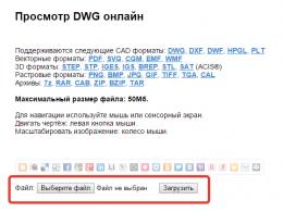
When buying a flash drive, many people ask themselves the question: "how to choose the right flash drive." Of course, choosing a flash drive is not so difficult if you know exactly for what purposes it is purchased. In this article I will try to give a complete answer to the question posed. I decided to write only about what to look for when buying.
A flash drive (USB drive) is a drive designed to store and transfer information. The flash drive works very simply without batteries. You just need to connect it to USB port your PC.
1. Flash drive interface
On the this moment There are 2 interfaces: USB 2.0 and USB 3.0. If you decide to buy a USB flash drive, then I recommend taking a USB 3.0 USB flash drive. This interface was made recently, its main feature is a high data transfer rate. We'll talk about speeds a little later.
This is one of the main parameters that you need to look at first. Now flash drives are sold from 1 GB to 256 GB. The cost of a flash drive will directly depend on the amount of memory. Here you need to immediately decide for what purpose a flash drive is bought. If you are going to store text documents, then 1 GB is enough. For downloading and transferring movies, music, photos, etc. you need to take the more, the better. To date, the most popular are flash drives with a capacity of 8GB to 16GB.
3. Body material

The body can be made of plastic, glass, wood, metal, etc. Flash drives are mostly made of plastic. There is nothing I can advise here, it all depends on the preferences of the buyer.
4. Transfer rate
Earlier I wrote that there are two standards USB 2.0 and USB 3.0. Now I will explain how they differ. The USB 2.0 standard has a read speed of up to 18 Mbps and a write speed of up to 10 Mbps. The USB 3.0 standard has a read speed of 20-70 Mbps, and a write speed of 15-70 Mbps. Here, I think, nothing needs to be explained.

Now in stores you can find flash drives of different shapes and sizes. They can be in the form of jewelry, fancy animals, etc. Here I would advise taking flash drives that have a protective cap.
6. Password protection
There are flash drives that have a password protection feature. Such protection is carried out using a program that is located in the flash drive itself. The password can be set both on the entire flash drive, and on part of the data in it. Such a flash drive will primarily be useful to people who transfer corporate information in it. According to the manufacturers, if you lose it, you don't have to worry about your data. Not so simple. If such a flash drive falls into the hands of an understanding person, then hacking it is just a matter of time.
Such flash drives look very beautiful, but I would not recommend buying them. Because they are very fragile and often break in half. But if you are a neat person, then feel free to take it.
Conclusion
Nuances, as you noticed, a lot. And this is just the tip of the iceberg. In my opinion, the most important parameters when choosing: the standard of a flash drive, the volume and speed of writing and reading. And everything else: design, material, options - this is just a personal choice of everyone.Good afternoon my dear friends. In today's article, I want to talk about how to choose the right mouse pad. When buying a rug, many do not attach any importance to this. But as it turned out, this moment needs to be given special attention, because. mat determine one of the indicators of comfort while working at a PC. For an avid gamer, choosing a rug is a completely different story. Consider what options for mouse pads have been invented today.

Mat options
1. Aluminum2. Glass
3. Plastic
4. Rubberized
5. Double sided
6. Helium
And now I would like to talk about each species in more detail.
1. First, I want to consider three options at once: plastic, aluminum and glass. These mats are very popular with gamers. For example, plastic mats are easier to find commercially. On such mats, the mouse glides quickly and accurately. And most importantly, these mats are suitable for both laser and optical mice. Aluminum and glass mats will be a little more difficult to find. And yes, they will cost a lot. The truth is for what - they will serve for a very long time. Rugs of these types have small flaws. Many people say that they rustle and feel a little cool to the touch during operation, which may cause discomfort for some users.

2. Rubberized (rag) mats have a soft glide, but the accuracy of their movements is worse. For ordinary users such a rug will be just right. Yes, and they are much cheaper than the previous ones.

3. Double-sided mousepads are, in my opinion, a very interesting kind of mousepads. As the name implies, these rugs have two sides. As a rule, one side is high-speed, and the other is high-precision. It happens that each side is designed for a certain game.

4. Helium pads have a silicone cushion. She allegedly supports her hand and relieves tension from it. For me personally, they were the most uncomfortable. By appointment, they are designed for office workers, since they sit at the computer all day. For ordinary users and gamers, these mats are not suitable. The mouse slides very poorly on the surface of such rugs, and their accuracy is not the best.

Mat sizes
There are three types of rugs: large, medium and small. It all depends on the taste of the user. But as is commonly believed, large rugs are well suited for games. Small and medium ones are taken mainly for work.Rugs design
In this regard, there are no restrictions. It all depends on what you want to see on your rug. The blessing now on rugs that only do not draw. The most popular are the logos of computer games such as DotA, Warcraft, ruler, etc. But if it happened that you could not find a rug with the pattern you need, do not be upset. Now you can order a print on the rug. But such rugs have a minus: when printing is applied to the surface of the rug, its properties deteriorate. Design for quality.
 On this I want to end the article. From myself I wish to make you right choice and be happy with it.
Who does not have a mouse or wants to replace it with another, I advise you to look at the article:.
Monoblocks from Microsoft replenished new model monoblock called Surface Studio. Microsoft presented its new product recently at an exhibition in New York.

On a note! I wrote an article a couple of weeks ago where I reviewed the Surface monoblock. This monoblock was presented earlier. Click on to view the article.
Design
Microsoft calls its new product the thinnest monoblock in the world. With a weight of 9.56 kg, the thickness of the display is only 12.5 mm, the other dimensions are 637.35x438.9 mm. The display dimensions are 28 inches with a resolution greater than 4K (4500x3000 pixels), aspect ratio 3:2.
On a note! The display resolution of 4500x3000 pixels corresponds to 13.5 million pixels. This is 63% more than 4K resolution.
The monoblock display itself is touch-sensitive, enclosed in an aluminum case. On such a display, it is very convenient to draw with a stylus, which ultimately opens up new possibilities for using a monoblock. In my opinion, this monoblock model will appeal to creative people (photographers, designers, etc.).

On a note! For people creative professions I advise you to look at the article where I considered monoblocks of similar functionality. Click on the selected one: .
To everything written above, I would add that the main feature of the monoblock will be its ability to instantly turn into a tablet with a huge work surface.

On a note! By the way, Microsoft has another amazing candy bar. To find out about it, go to.
Specifications
I will present the characteristics in the form of a photograph.
From the periphery, I note the following: 4 USB ports, a Mini-Display Port connector, an Ethernet network port, a card-reader, a 3.5 mm audio jack, a 1080p webcam, 2 microphones, a 2.1 Dolby Audio Premium audio system, Wi-Fi and Bluetooth 4.0. It also supports Xbox wireless controllers.


Price
When buying a monoblock, it will be installed with Windows 10 Creators Update. This system due out in the spring of 2017. In this operating system there will be an updated Paint, Office, etc. The price of a monoblock will be from $ 3,000.Dear friends, write in the comments what you think about this monoblock, ask your questions. I'll be glad to chat!
OCZ has demonstrated new VX 500 SSDs. These drives will be equipped with Serial ATA 3.0 interface and are made in 2.5-inch form factor.

On a note! For those who are interested in how SSD drives work and how long they live, you can read in an article I wrote earlier:.The novelties are made using 15-nanometer technology and will be equipped with Tochiba MLC NAND flash memory microchips. The controller in SSD drives will be used by Tochiba TC 35 8790.
The VX 500 drive lineup will consist of 128GB, 256GB, 512GB and 1TB. According to the manufacturer, the sequential read speed will be 550 Mb/s (this is for all drives in this series), but the write speed will be from 485 Mb/s to 512 Mb/s.

The number of input / output operations per second (IOPS) with data blocks of 4 KB in size can reach 92,000 when reading, and 65,000 when writing (this is all arbitrary).
The thickness of OCZ VX 500 drives will be 7 mm. This will allow them to be used in ultrabooks.


Prices of new products will be as follows: 128 GB - $ 64, 256 GB - $ 93, 512 GB - $ 153, 1 TB - $ 337. I think in Russia they will cost more.
Lenovo has unveiled its new IdeaCentre Y910 gaming all-in-one at Gamescom 2016.

On a note! Earlier, I wrote an article where I already considered gaming monoblocks from different manufacturers. This article can be viewed by clicking on this one.

The novelty from Lenovo received a 27-inch frameless display. The display resolution is 2560x1440 pixels (this is QHD format), the refresh rate is 144 Hz, and the response time is 5 ms.

The monoblock will have several configurations. The maximum configuration includes a 6th generation processor Intel Core i7 volume hard drive up to 2 TB or 256 GB. Volume random access memory equals 32 GB DDR4. Responsible for graphics NVIDIA graphics card GeForce GTX 1070 or GeForce GTX 1080 with Pascal architecture. Thanks to such a video card, it will be possible to connect a virtual reality helmet to the monoblock.
From the periphery of a monoblock, I would single out a Harmon Kardon audio system with 5-watt speakers, a Killer DoubleShot Pro Wi-Fi module, a webcam, USB ports 2.0 and 3.0, HDMI connectors.

In the basic version, the IdeaCentre Y910 monoblock will be available in September 2016 at a price of 1800 euros. But the monoblock with the version of "VR-ready" will appear in October at a price of 2200 euros. It is known that this version will have a GeForce GTX 1070 graphics card.
MediaTek has decided to upgrade its Helio X30 mobile processor. So now the developers from MediaTek are designing a new mobile processor called Helio X35.

I would like to briefly talk about Helio X30. This processor has 10 cores, which are combined into 3 clusters. Helio X30 has 3 variations. The first - the most powerful - consists of Cortex-A73 cores with a frequency of up to 2.8 GHz. There are also blocks with Cortex-A53 cores with a frequency of up to 2.2 GHz and Cortex-A35 with a frequency of 2.0 GHz.

The new Helio X35 processor also has 10 cores and is being created using 10nm technology. The clock frequency in this processor will be much higher than that of its predecessor and ranges from 3.0 Hz. The novelty will allow you to use up to 8 GB LPDDR4 RAM. The Power VR 7XT controller will most likely be responsible for the graphics in the processor.
The station itself can be seen in the photographs in the article. In them we can observe the drive bays. One bay with a 3.5" jack and the other with a 2.5" jack. Thus, it will be possible to connect to the new station as solid state drive(SSD) and HDD(HDD).

The dimensions of the Drive Dock station are 160x150x85mm, and the weight is no less than 970 grams.
Many people probably have a question about how the Drive Dock connects to a computer. The answer is: this happens through a USB 3.1 Gen 1 port. According to the manufacturer, the sequential read speed will be 434 Mb / s, and in write mode (serial) 406 Mb / s. The novelty will be compatible with Windows and Mac OS.

This device will be very useful for people who work with photo and video materials at a professional level. The Drive Dock can also be used to backups files.
The price for a new device will be acceptable - it is $ 90.
On a note! Previously, Renduchinthala worked at Qualcomm. And since November 2015, he moved to a competing company Intel.

In his interview, Renduchintala did not talk about mobile processors, but only said the following, and I quote: "I prefer to talk less and do more."
Thus, the top manager of Intel made an excellent intrigue with his interview. We just have to wait for more announcements in the future.
1982 AMD Am 286™
This processor was produced under license from Intel and had several interesting features, such as EMS emulation, as well as the ability to exit protected mode, which 286 "e Intel processors did not have. Specifications: clock frequency: 12-16 MHz.
198? AMD Am 386™ DX
Almost a complete analogue of the Intel-ovskoy "troika". Codename: P9. Those. specifications: 275,000 transistors; clock frequency: 16-32 MHz; 32-bit processor; data bus 32-bit (16-32MHz); address bus 32-bit; total bit depth: 32.
19?? AMD Am 386™ SX
low-end AMD version Am 386™ DX. Codename: P9. Those. specifications: 275,000 transistors; clock frequency: 16-32 MHz; 32-bit processor; data bus 16-bit (16-32MHz); address bus 24-bit; total bit depth: 16.
19?? AMD Am 486™ DX
Processor with built-in L1 cache and math coprocessor (FPU). Slightly behind in performance from a similar processor from Intel. Codename: P4 :) Tech. characteristics: 1.25 million transistors; clock frequency: 25-50 MHz; first level cache: 8 KB; second level cache motherboard(up to 512 Kb); 32-bit processor; data bus 32-bit (20-50 MHz); address bus 32-bit; total bit depth: 32.
199? AMD Am 486™ DX2
Fully 32-bit processor. Codename: P24. Specifications: 1.25 million transistors; clock frequency: 50-66 MHz; first level cache: 8 KB; second-level cache on the motherboard (up to 512 KB); 32-bit processor; data bus 32-bit (25-33 MHz); address bus 32-bit; total bit depth: 32.
199? AMD Am 486™ DX4
The latest "four" from AMD with an increased clock speed. Codename: P24C. Specifications: 1.25 million transistors; clock frequency: 75-120 MHz; first level cache: 8 KB; second-level cache on the motherboard (up to 512 KB); 32-bit processor; data bus 32-bit (25-40 MHz); address bus 32-bit; total bit depth: 32.
1995 AMD Am 586™
5th generation processor with integrated power management. Designed for installation on old motherboards (for "fours"). Code name: X5. Specifications: 1.6 million transistors; clock frequency: 133 MHz; first-level cache: 16 KB; second-level cache on the motherboard (up to 512 Kb); 32-bit processor; 32-bit data bus (33 MHz); 32-bit address bus; total bit width: 32.
1996 AMD K5™ (SSA5)
These processors are based on the x86-to-RISC86 architecture, which is fundamentally different from the architecture used in Intel Pentium processors, but they are installed in the same Socket 7 socket on motherboards and are fully compatible with Pentium processors. The first processors based on the SSA / 5 core were unfinished and did a disservice to the real K5, which came out later. These processors were labeled with a PR rating rather than the actual frequency. Codename: SSA5. Those. characteristics: 4.3 million transistors; production technology: 0.5 microns; clock frequency: 75-100 MHz; first level cache: 24 KB (8 KB for data and 16 KB for instructions); second-level cache on the motherboard (up to 1 MB); 64-bit processor; data bus 64-bit (50-66 MHz); address bus 32-bit; total bit depth: 32; socket 7 connector.
1996 AMD K5™ (5k86)
This processor showed excellent performance in office applications, but had a weak FPU, however, like the previous one. A PR rating was also used to label these processors. Codename: 5k86. Those. characteristics: 4.3 million transistors; production technology: 0.35 microns; clock frequency: 90-133 MHz; first level cache: 24 KB (8 KB for data and 16 KB for instructions); second-level cache on the motherboard (up to 1 MB); 64-bit processor; data bus 64-bit (60-66 MHz); address bus 32-bit; total bit depth: 32; socket 7 connector.
1997 AMD K6®
A processor built using x86-to-RISC86 technology can execute up to 6 RISC86 instructions simultaneously. It is installed in Socket 7 and can be used in boards designed for Pentium processors. Unlike its fellow Pentium MMX and Cyrix 6x86MX processors, it is software compatible with the Pentium Pro processor and works with MMX instructions, which makes it comparable to Intel's Pentium II processor. It was created based on the design of the 686 processor from the NexGen company acquired by AMD. Codename: K6. Those. characteristics: 888 million transistors; production technology: 0835 microns; clock frequency: 166-233 MHz; first level cache: 64 KB (32 KB for data and 32 KB for instructions); second-level cache on the motherboard (up to 1 MB); 64-bit processor; data bus 64-bit (66 MHz); address bus 32-bit; total bit depth: 32; socket 7 connector.
1997 AMD K6® (Little Foot)
This processor was produced on a 0.25 micron process and had a higher clock speed than its predecessor. Codename: Little Foot. Those. characteristics: 8.8 million transistors; production technology: 0.25 microns; clock frequency: 233-300 MHz; first level cache: 64 KB (32 KB for data and 32 KB for instructions); second-level cache on the motherboard (up to 1 MB); 64-bit processor; data bus 64-bit (66 MHz); address bus 32-bit; total bit depth: 32; socket 7 connector.
1998 AMD K6®-2
The main improvements in this processor are support for an additional 3DNow! instruction set, which significantly improves performance in optimized programs and games, as well as a 100 MHz system bus. Codename: Chomper XT. Those. characteristics: 9.3 million transistors; production technology: 0.25 microns; clock frequency: 266-550 MHz; first level cache: 64 KB (32 KB for data and 32 KB for instructions); second-level cache on the motherboard (up to 1 MB); 64-bit processor; data bus 64-bit (66-100 MHz); address bus 32-bit; total bit depth: 32; socket 7 connector.
1999 AMD K6®-III
The first processor from AMD to have L2 cache integrated into the core. They are K6-2 with 256 KB L2 cache on the chip, operating at the same frequency as the processor core. Recommended for installation on Super Socket 7 motherboards with AGP support. Codename: Sharptooth. Those. characteristics: 21.3 million transistors; production technology: 0.25 microns; clock frequency: 350-500 MHz; first level cache: 64 KB (32 KB for data and 32 KB for instructions); 256 KB L2 cache (full speed); third-level cache on the motherboard (up to 3 MB); 64-bit processor; data bus 64-bit (100 MHz); address bus 32-bit; total bit depth: 32; Super Socket 7 connector.
1999 Mobile AMD K6®-2
Mobile version of K6®-2 with PowerNow!™ technology designed to reduce processor power consumption. Those. characteristics: 9.3 million transistors; production technology: 0.25 microns; clock frequency: 300-500 MHz; first level cache: 64 KB (32 KB for data and 32 KB for instructions); second-level cache on the motherboard (up to 2 MB); 64-bit processor; data bus 64-bit (100 MHz); address bus 32-bit; total bit depth: 32; socket 7 connector.

1999 AMD Athlon™
The first processor whose architecture and interface is different from Intel. After its release, Intel's positions were somewhat shaken, because it demonstrated greater performance in most applications than Pentium !!! at the same clock speeds. It has an extended instruction set Enhanced 3DNow!. Codename: K7, K75 (aluminum connections), K76 (copper connections). Those. characteristics: 22 million transistors; production technology: 0.25-0.18 microns; clock frequency: 500-1000 MHz; first level cache: 128 KB (64 KB for data and 64 KB for instructions); second-level cache 512 KB, operating at 1/2, 2/5 or 1/3 of the processor frequency; processor bus - Alpha EV-6 200 MHz (DDR 100x2); total bit depth: 32; Slot A connector.
2000 AMD Athlon™ Thunderbird
This processor is manufactured in 0.18 micron technology using copper connection technology. It was originally released in the Slot A form factor, later Socket A. The chip integrated 256 KB of L2 cache, running at the processor frequency. Codename: Thunderbird. Those. characteristics: production technology: 0.18 microns; clock frequency: 600-1400 MHz; first level cache: 128 KB (64 KB for data and 64 KB for instructions); 256 KB L2 cache (full speed); processor bus - Alpha EV-6 200-266MHz (DDR 100x2-133x2); total bit depth: 32; Slot A connector, later Socket A.
2000 AMD Duron™ (Spitfire)
Low-End version of Athlon™ Thunderbird with L2 cache trimmed to 64 KB. Carries Celeron to smithereens, although it has a lower price. Codename: Spitfire. Those. characteristics: 25 million transistors; production technology: 0.18 microns; clock frequency: 600-950 MHz; first level cache: 128 KB (64 KB for data and 64 KB for instructions); 64 KB L2 cache (full speed); processor bus - Alpha EV-6 200 MHz (DDR 100x2); total bit depth: 32; Socket A connector.
2000 AMD K6®-2+
The latest processor in the K6® family features a 0.18 micron process, 128KB L2 cache and PowerNow!™ technology. Those. characteristics: production technology: 0.18 microns; clock frequency: 450-550 MHz; first level cache: 64 KB (32 KB for data and 32 KB for instructions); second-level cache on the motherboard (up to 3 MB); 64-bit processor; data bus 64-bit (95-100 MHz); address bus 32-bit; total bit depth: 32; Super Socket 7 connector.
2001 Mobile AMD Duron™
The mobile version of Duron with PowerNow!™ technology. Those. characteristics: production technology: 0.18 microns; clock frequency: 700-950 MHz; first level cache: 128 KB (64 KB for data and 64 KB for instructions); 64 KB L2 cache (full speed); processor bus - Alpha EV-6 200 MHz (DDR 100x2); total bit depth: 32.
2001 AMD Athlon™ 4
Mobile Athlon™ powered by the new Palomino core, which adds support for Intel's SSE instruction set. Codename: Palomino. Those. characteristics: production technology: 0.18 microns; clock frequency: 950-1400 MHz; first level cache: 128 KB (64 KB for data and 64 KB for instructions); 256 KB L2 cache (full speed); processor bus - Alpha EV-6 266 MHz (DDR 133x2); total bit depth: 32; Socket A connector.
2001 AMD Athlon™ MP
The first processor from AMD, designed to work in dual-processor systems, is made on the Palomino core. The marking of the first processors indicated the real clock frequency, and in later ones the performance index. Codename: Palomino. Those. characteristics: production technology: 0.18 microns; clock frequency: 1000-1667 MHz; first level cache: 128 KB (64 KB for data and 64 KB for instructions); 256 KB L2 cache (full speed); processor bus - Alpha EV-6 266 MHz (DDR 133x2); total bit depth: 32; Socket A connector.
2001 AMD Duron™ (Morgan)
This Duron is made on the Morgan core - a stripped-down version of Palomino (L2 cache is not 256, but 64 KB). Codename: Morgan. Those. characteristics: 25.18 million transistors; production technology: 0.18 microns; clock frequency: 1000-1300 MHz; first level cache: 128 KB (64 KB for data and 64 KB for instructions); 64 KB L2 cache (full speed); processor bus - Alpha EV-6 200 MHz (DDR 100x2); total bit depth: 32; Socket A connector.
2001 AMD Athlon™ XP
A version of the Palomino core processor for desktop computers. When marking these processors, not the real clock speed is used, but the performance index, that is, it shows which Pentium 4 this processor corresponds to. For example Athlon XP 2000+ runs at 1667 MHz. Unlike AMD K5, this is a real indicator and Athlon XP 1900+ is really not inferior to P4 1900 MHz, and even surpasses it in some applications. Those. characteristics: production technology: 0.18 microns; clock frequency: 1333-1800MHz; first level cache: 128 KB (64 KB for data and 64 KB for instructions); 256 KB L2 cache (full speed); processor bus - Alpha EV-6 266 MHz (DDR 133x2); total bit depth: 32; Socket A connector.
2002 AMD Athlon™ XP (Thoroughbred)
Continued development of the Athlon XP processor. Unlike the previous one, it is made in 0.13 microns of those. process and the marking is applied not to the crystal, but to a special plate. The processor core has become somewhat stronger. When marking these processors, it is also not the real clock frequency that is used, but the performance index. Codename: Thoroughbred. Those. characteristics: production technology: 0.13 microns; clock frequency: 1466-2250MHz; first level cache: 128 KB (64 KB for data and 64 KB for instructions); 256 KB L2 cache (full speed); processor bus - Alpha EV-6 266/333MHz (DDR 133x2/166x2); total bit depth: 32; Socket A connector.
2003 AMD Athlon™ XP (Barton)
The latest processor from the Athlon XP family. Made according to 0.13 microns of those. process and the second level cache has been increased to 512 KB. When marking these processors, it is also not the real clock frequency that is used, but the performance index. Codename: Barton. Those. characteristics: production technology: 0.13 microns; clock frequency: 1833-2166MHz; first level cache: 128 KB (64 KB for data and 64 KB for instructions); 512 KB L2 cache (full speed); processor bus - Alpha EV-6 333MHz (DDR 166x2); total bit depth: 32; Socket A connector.
Continuing the theme of the first article - the history of the evolution of processors from the end of the 20th century to the beginning of the 21st century.
Many processors in the 80s used the CISC (Complex instruction set computing) architecture. The chips were quite complex and expensive, and also not powerful enough. There was a need to modernize production and increase the number of transistors.
RISC architecture
In 1980, the Berkeley RISC project was launched, led by American engineers David Patterson and Carlo Sequin. RISC (restricted instruction set computer) is a processor architecture with increased performance due to simplified instructions.
Berkeley RISC project leaders - David Patterson and Carlo Sequin
After several years of fruitful work, several samples of processors with a reduced instruction set appeared on the market. Each instruction of the RISC platform was simple and executed in one clock cycle. Many more general purpose registers were also present. In addition, pipelining with simplified instructions was used, which made it possible to effectively increase the clock frequency.
RISC I came out in 1982 and contained over 44,420 transistors. It had only 32 instructions and ran at 4 MHz. The next RISC II had 40,760 transistors, used 39 instructions, and was faster.

RISC II processor
MIPS Processors: R2000, R3000, R4000, and R4400
The architecture of MIPS processors (Microprocessor without Interlocked Pipeline Stages) provided for the presence of auxiliary blocks in the crystal. MIPS used an elongated conveyor.
In 1984, a group of researchers led by American scientist John Hennessy founded a company that designs microelectronic devices. MIPS licensed microprocessor architecture and IP cores for devices smart home, network and mobile applications. In 1985, the company's first product was released - the 32-bit R2000, which was finalized in 1988 in the R3000. The updated model had support for multiprocessing, cache memory for instructions and data. The processor has found application in the SG-series of workstations from various companies. The R3000 also became the basis of the Sony PlayStation game console.

Processor R3000
In 1991, the new generation R4000 line was released. This processor had a 64-bit architecture, built-in coprocessor and ran at a clock frequency of 100 MHz. The internal cache memory was 16 KB (8 KB instruction cache and 8 KB data cache).
A year later, a modified version of the processor, the R4400, was released. In this model, the cache has increased to 32 KB (16 KB cache commands and 16 KB cache data). The processor could operate at a frequency of 100 MHz - 250 MHz.
MIPS processors: R8000 and R10000
In 1994, the first processor with a superscalar implementation of the MIPS architecture, the R8000, appeared. The data cache capacity was 16 KB. This CPU had a high data access bandwidth (up to 1.2 Gb / s) combined with a high speed of execution of operations. The frequency reached 75 MHz - 90 MHz. 6 schemes were used: an integer instruction device, a floating point instruction device, three secondary RAM cache descriptors, and an ASIC cache controller.

Processor R8000
In 1996, a modified version was released - R10000. The processor included 32 KB of primary data and instruction cache. The CPU worked at a frequency of 150 MHz - 250 MHz.
In the late 1990s, MIPS began selling licenses for the 32-bit and 64-bit MIPS32 and MIPS64 architectures.
SPARC processors
The ranks of processors were replenished with products from Sun Microsystems, which developed the scalable architecture SPARC (Scalable Processor ARChitecture). The first processor of the same name was released in the late 80s and was called SPARC V7. Its frequency reached 14.28 MHz - 40 MHz.
In 1992, the next 32-bit version called SPARC V8 appeared, on the basis of which the microSPARC processor was created. The clock frequency was 40 MHz - 50 MHz.
Texas Instruments, Fujitsu, Philips, and others have collaborated with Sun Microsystems to create the next generation of the SPARC V9 architecture. The platform expanded to 64 bits and was superscalar with a 9-stage pipeline. SPARC V9 provided for the use of a cache memory of the first level, divided into instructions and data (each with a capacity of 16 KB), as well as a second level with a capacity of 512 KB - 1024 KB.

UltraSPARC III processor
StrongARM processors
In 1995, a project was launched to develop the StrongARM microprocessor family, which implemented the ARM V4 instruction set. These CPUs were a classic scalar architecture with a 5-stage pipeline, including memory management units and supporting 16 KB instruction and data caches each.

StrongARM SA-110
And already in 1996, the first StrongARM-based processor, the SA-110, was released. It ran at clock speeds of 100 MHz, 160 MHz, or 200 MHz.
The SA-1100, SA-1110 and SA-1500 models also entered the market.

SA-110 processor in the Apple MessagePad 2000
POWER, POWER2 and PowerPC processors
In 1985, IBM began developing the next generation RISC architecture as part of the America Project. The development of the POWER (Performance Optimization With Enhanced RISC) processor and the instruction set for it lasted 5 years. It was very productive, but consisted of 11 different microcircuits. And so in 1992 another version of the processor came out that fit in one chip.

Chipset
In 1991, the PowerPC architecture (abbreviated as PPC) was developed by the joint efforts of an alliance of IBM, Apple and Motorola. It consisted of the core feature set of the POWER platform, and also supported dual mode operation and was backwards compatible with 32-bit operation mode for the 64-bit version. The main purpose was personal computers.
The PowerPC 601 processor was used in the Macintosh.

PowerPC processor
In 1993, the POWER2 was introduced with an extended instruction set. The processor clock speed ranged from 55 MHz to 71.5 MHz, and the data and instruction cache was 128-256 KB and 32 KB. The processor chips (there were 8 of them) contained 23 million transistors, and it was manufactured using 0.72-micrometer CMOS technology.
In 1998, IBM released the third series of 64-bit POWER3 processors fully compliant with the PowerPC standard.
In the period from 2001 to 2010, POWER4 models (up to eight parallel commands), dual-core POWER5 and POWER6, and four to eight-core POWER7 were released.
Alpha 21064A processors
In 1992, Digital Equipment Corporation (DEC) released the Alpha 21064 (EV4) processor. It was a 64-bit superscalar crystal with a pipelined architecture and a clock speed of 100 MHz - 200 MHz. Manufactured according to the 0.75-micron process technology, with an external 128-bit processor bus. There was 16 KB of cache memory (8 KB of data and 8 KB of instructions).
The next model in the series was the 21164 (EV5) processor, which was released in 1995. It had two integer blocks and already had three levels of cache memory (two in the processor, the third - external). The first level cache was divided into a data cache and an instruction cache of 8 KB each. The volume of cache memory of the second level was 96 KB. The processor clock speed varied from 266 MHz to 500 MHz.

DEC Alpha AXP 21064
In 1996, the Alpha 21264 (EV6) processors were released with 15.2 million transistors, manufactured using a 15.2-micron process technology. Their clock frequency ranged from 450 MHz to 600 MHz. Integer blocks and load/save blocks were combined into a single Ebox module, and floating point blocks into an Fbox module. The first-level cache retained the division into memory for instructions and for data. The volume of each part was 64 Kb. The amount of cache memory in the second level was from 2 MB to 8 MB.
Compaq bought DEC in 1999. As a result, most of the production of products using Alpha was transferred to API NetWorks, Inc.
Intel P5 and P54C processors
Based on the layout of Vinod Dham, the fifth generation processor was developed, codenamed P5. In 1993, the CPU went into production under the name Pentium.
Processors based on the P5 core were manufactured using an 800-nanometer process technology using bipolar BiCMOS technology. They contained 3.1 million transistors. The Pentium had a 64-bit data bus, superscalar architecture. There was separate caching program code and data. A 16 KB L1 cache was used, divided into 2 segments (8 KB for data and 8 KB for instructions). The first models were with frequencies of 60 MHz - 66 MHz.

Intel Pentium processor
In the same year, Intel launched the P54C processors. The production of new processors was transferred to the 0.6-micron process technology. The speed of the processors was 75 MHz, and since 1994 - 90 MHz and 100 MHz. A year later, the P54C (P54CS) architecture was switched to the 350nm process technology and the clock frequency increased to 200MHz.
In 1997, the P5 received Last update- P55C (Pentium MMX). Added support for the MMX (MultiMedia eXtension) command set. The processor consisted of 4.5 million transistors and is manufactured using advanced 280nm CMOS technology. The size of the first level cache has increased to 32 KB (16 KB for data and 16 KB for instructions). The processor frequency reached 233 MHz.
AMD K5 and K6 Processors
In 1995, AMD released the K5 processor. The architecture was a RISC core, but worked with complex CISC instructions. The processors were manufactured using a 350- or 500-nanometer process technology, with 4.3 million transistors. All K5s had five integer units and one floating point unit. The size of the instruction cache was 16 KB, and the data cache was 8 KB. The clock frequency of the processors ranged from 75 MHz to 133 MHz.

AMD K5 processor
Under the K5 brand, two variants of the SSA / 5 and 5k86 processors were produced. The first worked at frequencies from 75 MHz to 100 MHz. The 5k86 processor ran at frequencies from 90 MHz to 133 MHz.
In 1997, the company introduced the K6 processor, which had a significantly different architecture from the K5. The processors were manufactured using a 350-nanometer process technology, included 8.8 million transistors, supported reordering of instructions, the MMX instruction set, and a floating point unit. The crystal area was 162 mm². The L1 cache was 64 KB (32 KB data and 32 KB instructions). The processor worked at a frequency of 166 MHz, 200 MHz and 233 MHz. The system bus frequency was 66 MHz.
In 1998, AMD released chips with an improved K6-2 architecture, with 9.3 million transistors manufactured using a 250-nanometer process technology. The maximum chip frequency was 550 MHz.

AMD K6 processor
In 1999, the third generation came out - the K6-III architecture. The crystal retained all the features of the K6-2, but at the same time there was a built-in 256 KB L2 cache. The volume of the cache of the first level was 64 KB.
AMD K7 processors
In the same 1999, K6 processors were replaced by K7 processors. They were produced in 250nm technology with 22 million transistors. The CPU had new block integer computing (ALU). The EV6 system bus provided data transfer on both edges of the clock signal, which made it possible to obtain an effective frequency of 200 MHz at a physical frequency of 100 MHz. The first level cache was 128 KB (64 KB instructions and 64 KB data). The second level cache reached 512 KB.

AMD K7 processor
Somewhat later, crystals appeared based on the core of Orion. They were manufactured using the 180nm process technology.
The release of the Thunderbird kernel brought unusual changes to processors. The L2 cache was moved directly to the processor core and ran at the same frequency as it. The cache was 384 KB effective (128 KB L1 cache and 256 KB L2 cache). The clock frequency of the system bus has increased - now it operates at a frequency of 133 MHz.
Intel P6 processors
The P6 architecture replaced the P5 in 1995. The processor was superscalar and supported reordering of operations. The processors used a dual independent bus, which greatly increased the memory bandwidth.
Also in 1995, the next generation Pentium Pro processors were introduced. The crystals operated at a frequency of 150 MHz - 200 MHz, had 16 KB of L1 cache and up to 1 Mb of L2 cache.

Intel Pentium Pro Processor
In 1999, the first Pentium III processors were introduced. They were based on a new generation of the P6 kernel called Katmai, which were modified versions of Deschutes. Support for SSE instructions has been added to the kernel, and the mechanism for working with memory has also been improved. The clock frequency of Katmai processors reached 600 MHz.
In 2000, the first Pentium 4 processors with the Willamette core came out. The effective system bus frequency was 400 MHz (physical frequency - 100 MHz). The cache data of the first level reached 8 KB, and the cache memory of the second level - 256 KB.
The next core of the line was Northwood (2002). The processors contained 55 million transistors and were manufactured using a new 130nm CMOS technology with copper connections. The system bus frequency was 400 MHz, 533 MHz, or 800 MHz.

Intel Pentium 4
In 2004, the production of processors was again transferred to thinner technological standards - 90 nm. Pentium 4 came out on the Prescott core. The first level data cache has increased to 16 KB, and the second level cache has reached 1 MB. The clock frequency was 2.4 GHz - 3.8 GHz, the system bus frequency was 533 MHz or 800 MHz.
The last core used in Pentium 4 processors was the single-core Cedar Mill. Produced according to a new process technology - 65 nm. There were four models: 631 (3 GHz), 641 (3.2 GHz), 651 (3.4 GHz), 661 (3.6 GHz).
Athlon 64 and Athlon 64 X2 processors
At the end of 2003, AMD released a new 64-bit K8 architecture built on a 130-nanometer process technology. The processor had an integrated memory controller and a HyperTransport bus. She worked at a frequency of 200 MHz. The new AMD products were called Athlon 64. The processors supported many instruction sets such as MMX, 3DNow!, SSE, SSE2 and SSE3.

Athlon 64 processor
In 2005, AMD processors called Athlon 64 X2 entered the market. These were the first dual-core desktop processors. The model was based on two cores made on a single chip. They shared a common memory controller, HyperTransport bus, and command queue.

Athlon 64 X2 processor
During 2005 and 2006, AMD released four generations of dual-core chips: three 90nm Manchester, Toledo, and Windsor cores, and a 65nm Brisbane core. The processors differed in L2 cache size and power consumption.
Intel Core processors
Pentium M processors provided greater performance than desktop processors based on the NetBurst microarchitecture. And so their architectural solutions became the basis for the Core microarchitecture, which was released in 2006. The first desktop quad-core processor was the Intel Core 2 Extreme QX6700 clocked at 2.67 GHz with 8 MB L2 cache.
First generation codename mobile processors Intel was Yonah. They were manufactured using a 65 nm process based on the Banias/Dothan Pentium M architecture with added LaGrande security technology. The processor could process up to four instructions per clock. The algorithm for processing 128-bit SSE, SSE2, and SSE3 instructions has been redesigned in Core. If earlier each command was processed in two cycles, now only one cycle was required for the operation.

Intel Core 2 Extreme QX6700
In 2007, the 45nm Penryn microarchitecture was released using lead-free Hi-k metal gates. The technology was used in the Intel Core 2 Duo processor family. Support for SSE4 instructions has been added to the architecture, and the maximum amount of L2 cache for dual-core processors has increased from 4 MB to 6 MB.

AMD Phenom II X6 processor
In 2008, the next generation architecture, Nehalem, was released. The processors have an integrated memory controller that supports 2 or 3 DDR3 SDRAM channels or 4 FB-DIMM channels. The FSB bus was replaced by a new QPI bus. The L2 cache has been reduced to 256 KB per core.

Intel Core i7
Soon, Intel moved the Nehalem architecture to a new 32nm process technology. This line of processors was named Westmere.
The first model of the new microarchitecture was Clarkdale, which has two cores and an integrated graphics core, produced on a 45-nm process technology.
AMD K10 processors
AMD has tried to keep up with Intel. In 2007, it released the x86 microprocessor architecture generation, the K10. Four processor cores were combined on one chip. In addition to L1 and L2 cache, the K10 models finally received 2MB L3. The size of the data and instruction cache of the 1st level was 64 KB each, and the cache of the 2nd level was 512 KB. There is also promising support for DDR3 memory controller. The K10 used two 64-bit controllers. Each processor core had a 128-bit floating point module. On top of that, the new processors worked through the HyperTransport 3.0 interface.
In 2007, with the K10 architecture, AMD's multi-core Phenom central processors were released, designed for use in stationary personal computers. Solutions based on K10 were produced on 65- and 45-nm process technology. V new version architecture (K10.5) the memory controller worked with DDR2 and DDR3 memory.

AMD Phenom processor
In 2011, the new Bulldozer architecture was released. Each module contained two cores with their own integer computation unit and level 1 cache. It supported 8 MB L3 cache, HyperTransport 3.1 buses, second-generation Turbo Core frequency increase technologies and AVX, SSE 4.1, SSE 4.2, AES instruction sets. Also, Bulldozer processors were endowed with a dual-channel DDR3 memory controller with an effective frequency of 1866 MHz.

AMD Bulldozer Processor
In 2013, the company introduced the next generation of processors - Piledriver. This model was an improved Bulldozer architecture. The branch prediction units have been improved, the performance of the floating point and integer calculations, as well as the clock frequency, have increased.
Looking through the history, you can trace the stages of development of processors, changes in their architecture, improvements in development technologies, and much more. Modern CPUs are different from those that came out before, but they also have common features.