How it works: microprocessor
You are currently using a computer or mobile device to read this thread. The computer or mobile device uses a microprocessor to perform these actions. The microprocessor is the heart of any device, server or laptop. There are many brands of microprocessors from many different manufacturers, but they all do pretty much the same thing and in much the same way.
Microprocessor- also known as a processor or central processing unit, is a computing engine that is manufactured on a single chip. The first microprocessor was the Intel 4004, which appeared in 1971 and was not as powerful. He could add and subtract, and that's only 4 bits at a time. The processor was amazing because it was made on a single chip. You will ask why? And I will answer: engineers at that time produced processors either from several chips or from discrete components (transistors were used in separate packages).
If you have ever wondered what a microprocessor does in a computer, what it looks like, or what its differences are compared to other types of microprocessors, then go under cat- there all the most interesting, and details.
Microprocessor Progress: Intel
The first microprocessor, which later became the heart of a simple home computer, was the Intel 8080, a complete 8-bit computer on a single chip that appeared in 1974. The first microprocessor caused a real surge in the market. Later in 1979, a new model was released - Intel 8088. If you are familiar with the PC market and its history, then you know that the PC market moved from Intel 8088 to Intel 80286, and that to Intel 80386 and Intel 80486, and then to Pentium, Pentium II, Pentium III and Pentium 4. These microprocessors are all made by Intel, and they are all improvements to the basic design of the Intel 8088. The Pentium 4 can execute any code, but it does it 5000 times faster.
In 2004, Intel introduced microprocessors with multiple cores and a million transistors, but even these microprocessors followed the same general rules as previously manufactured chips. Additional information in the table:
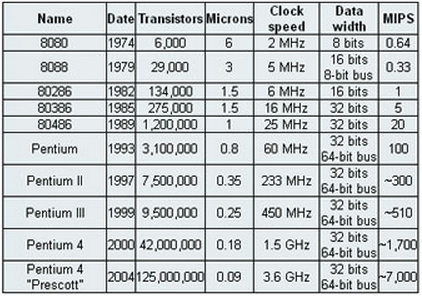
- date: is the year the processor was first introduced. Many processors were re-released at higher clock speeds and this continued for many years after the original release date.
- transistors: is the number of transistors on a chip. You can see that the number of transistors on a single chip has been steadily increasing over the years.
- Micron: width in microns of the smallest wire on the chip. For comparison, I can give a human hair, which has a thickness of about 100 microns. As the sizes got smaller and smaller, the number of transistors increased.
- Clock frequency: The maximum speed that the chip can reach. I will talk about the clock frequency a little later.
- Width (bus) data: is the width of the ALU (Arithmetic Logic Unit). An 8-bit ALU can add, subtract, multiply, etc. In many cases, the data bus is the same width as the ALU, but not always. The Intel 8088 was 16-bit and had an 8-bit bus, while current Pentium models are 64-bit.
- MIPS: this column in the table stands for displaying the number of operations per second. It is a unit of measure for microprocessors. Modern processors can do so many things that today's ratings presented in the table will lose all meaning. But you can feel the relative power of the microprocessors of those times
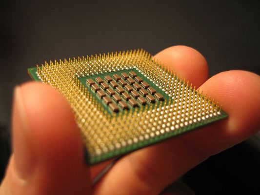
What is a chip?
The chip is also called an integrated circuit. This is usually a small, thin piece of silicon on which the transistors that make up the microprocessor have been engraved. A chip can be as small as one inch, but still contain tens of millions of transistors. Simpler processors may consist of several thousand transistors etched into a chip of just a few square millimeters.
How it works
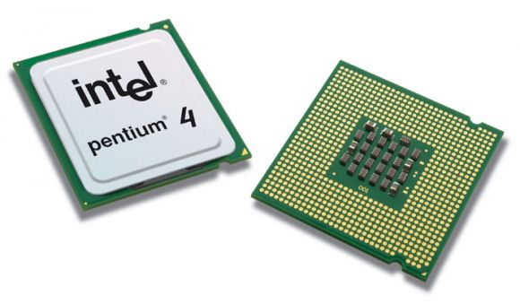
Intel Pentium 4
To understand how a microprocessor works, it would be helpful to look inside and learn about its innards. In the process, you can also learn about assembly language, the microprocessor's native language, and many things that engineers can do to increase the speed of a processor.
The microprocessor executes a collection of machine instructions that tell the processor what to do. Based on instructions, the microprocessor does three main things:
- Using its ALU (arithmetic logic unit), the microprocessor can perform mathematical operations. For example, addition, subtraction, multiplication and division. Modern microprocessors are capable of performing extremely complex operations.
- The microprocessor can move data from one memory location to another
- The microprocessor can make decisions and jump to a new set of instructions based on those decisions.
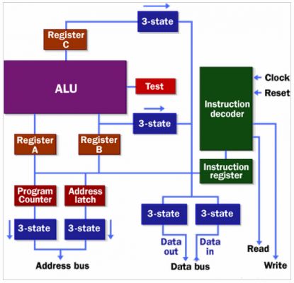
To put it bluntly, the microprocessor does complex things, but above I have described three main activities. The following diagram shows a very simple microprocessor capable of doing these three things. This microprocessor has:
- Address bus (8, 16, or 32 bits) that sends memory access
- Data bus (8, 16, or 32 bits) that sends data to or receives data from memory
- RD (read, read) and WR (write, write) tell the memory whether they want to set or get the addressed location
- Clock line that allows you to view the processor clock sequence
- Reset line that resets the program counter to zero and restarts execution
microprocessor memory
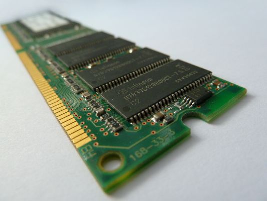
 Earlier we talked about address and data buses, as well as read and write lines. All this is connected to either RAM (Random Access Memory) or ROM (Read Only Memory or Read Only Memory, ROM) - usually both. In our example microprocessor, we have a wide address bus of 8 bits and the same wide data bus - also 8 bits. This means that the microprocessor can access 2^8 to 256 bytes of memory, and can read and write 8 bits of memory at a time. Let's assume that this simple microprocessor has 128 bytes of internal memory starting at address 0 and 128 bytes of RAM starting at address 128.
 RAM stands for read-only memory. The permanent memory chip is programmed with permanent preset preset bytes. The bus address tells the RAM chip which byte to reach and fit on the data bus. When the read line changes state, the ROM chip presents the selected byte to the data bus.
RAM stands for RAM, lol. RAM contains a byte of information, and the microprocessor can read or write to those bytes depending on whether the read or write line is signaling. One of the problems that can be found in today's chips is that they forget everything as soon as the energy is gone. Therefore, the computer must have RAM.
RAM chip or Read Only Memory (ROM) chip
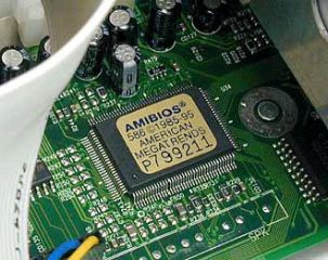
By the way, almost all computers contain some amount of RAM. On a personal computer, the read-only memory is called the BIOS (Basic Input/Output System). At startup, the microprocessor starts executing the instructions it finds in the BIOS. BIOS instructions, by the way, also perform their role: they perform a hardware check, and then all the information goes to the hard disk to create a boot sector. The boot sector is one small program, and the BIOS keeps it in memory after reading it from disk. The microprocessor then starts executing the boot sector instructions from RAM. The boot sector program will tell the microprocessor what else to take with it from the hard drive to RAM, and then it does all that, and so on. This is how the microprocessor loads and executes the entire operating system.
microprocessor instructions
Even the incredibly simple microprocessor I've just described will have a fairly large set of instructions that it can execute. The instruction collection is implemented as bit patterns, each of which has a different meaning when loaded into the instruction sector. People don't remember bit patterns particularly well, as it's a collection of short words. By the way, this set of short words is called the processor assembly language. The assembler can translate words into a bit pattern very easily, and then the assembler's effort will be put into memory for the microprocessor to execute.Here is a set of assembly language instructions:
- LOADA mem- load into register with memory address
- LOADB mem- load into register B from memory address
- CONB mem- load a constant value into register B
- SAVEB mem- save register B to memory address
- SAVEC mem- save register C to memory address
- ADD- add A and B and store the result in C
- SUB- subtract A and B and store the result in C
- MUL- multiply A and B and store the result in C
- DIV- split A and B and store the result in C
- COM- compare A and B and store the result in the test
- JUMP addr- go to address
- JEQ addr- jump if equal to solve
- JNEQ addr- jump if not equal to solve
- JG addr- jump if more, to solve
- JGE addr- jump if greater than or equal to to solve
- JL addr- jump if less to solve
- JLE addr- jump if less than or equal to to solve
- STOP- stop execution
The C compiler translates this C code into assembly language. Assuming that main memory starts at address 128 in this processor, and read-only memory (which contains the assembly language program) starts at address 0, then for our simple microprocessor, the assembler might look like this:
// Assume a is at address 128 // Assume F is at address 1290 CONB 1 // a=1;1 SAVEB 1282 CONB 1 // f=1;3 SAVEB 1294 LOADA 128 // if a > 5 the jump to 175 CONB 56 COM7 JG 178 LOADA 129 // f=f*a;9 LOADB 12810 MUL11 SAVEC 12912 LOADA 128 // a=a+1;13 CONB 114 ADD15 SAVEC 12816 JUMP 4 // loop back to if17 STOP
Read Only Memory (ROM)
So now the question is: "How do all these instructions integrate with ROM?". I will explain, of course: each of these assembly language instructions must be represented as a binary number. For simplicity, let's assume that each assembly language instruction assigns itself a unique number. For example, it will look like this:
- LOADA - 1
- LOADB - 2
- CONB - 3
- SAVEB - 4
- SAVEC mem - 5
- ADD - 6
- SUB - 7
- MUL - 8
- DIV - 9
- COM - 10
- JUMP addr - 11
- JEQ addr - 12
- JNEQ addr - 13
- JG addr - 14
- JGE addr - 15
- JL addr - 16
- JLE addr - 17
- STOP - 18
// Assume a is at address 128 // Assume F is at address 129Addr opcode/value0 3 // CONB 11 12 4 // SAVEB 1283 1284 3 // CONB 15 16 4 // SAVEB 1297 1298 1 // LOADA 1289 12810 3 // CONB 511 512 10 // COM13 14 // JG 1714 3115 1 // LOADA 12916 12917 2 // LOADB 12818 12819 8 // MUL20 5 // SAVEC 12921 12922 1 // LOADA 12823 12824 3 // CONB 125 // ADD27 5 // SAVEC 12828 12829 11 // JUMP 430 831 18 // STOP
You see that 7 lines of C code became 18 lines of assembler, and that all became 32 bytes in ROM.
Decoding
The decode instruction must turn each of the opcodes into a set of signals that will control various components within the microprocessor. Let's take the ADD instructions as an example and see what it has to do. So:
- 1. In the first cycle, it is necessary to load the instruction itself, so the decoder needs to: activate the buffer for the program counter with three states, activate the read line (RD), activate the data in the three states of the buffer in the instruction register
- 2. In the second cycle, the ADD instruction is decoded. Here you need to do very little: set the operation of the arithmetic logic unit (ALU) to register C
- 3. During the third cycle, the program counter is incremented (in theory this may overlap in the second cycle)
Let's come to the end
The number of transistors has a huge impact on processor performance. As you can see above, a typical Intel 8088 microprocessor could run 15 cycles. The more transistors, the higher the performance - it's simple. A large number of transistors also allows technology such as pipelining.
The pipeline architecture is made up of the execution of commands. It may take five cycles to execute one instruction, but there cannot be five instructions in different stages of execution at the same time. So it looks like one instruction completes each clock cycle.
All of these trends allow the number of transistors to grow, resulting in the multi-million dollar transistor heavyweights that are available today. Such processors can perform about a billion operations per second - just imagine. By the way, now many manufacturers have become interested in the release of 64-bit mobile processors, and obviously the next wave is coming, only this time the 64-bit architecture is the king of fashion. Maybe I will get to this topic in the near future and tell you how it actually works. On this, perhaps, everything for today. I hope you enjoyed it and learned a lot.